
|
시장보고서
상품코드
1630293
플라즈마 에칭 장비 : 시장 점유율 분석, 산업 동향 및 통계, 성장 예측(2025-2030년)Plasma Etching Equipment - Market Share Analysis, Industry Trends & Statistics, Growth Forecasts (2025 - 2030) |
||||||
■ 보고서에 따라 최신 정보로 업데이트하여 보내드립니다. 배송일정은 문의해 주시기 바랍니다.
가격
※ 부가세 별도
한글목차
영문목차
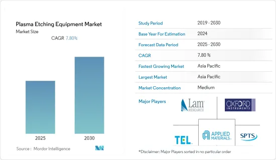
플라즈마 에칭 장비 시장은 예측 기간 동안 7.8%의 CAGR을 기록할 것으로 예상됩니다.
주요 하이라이트
- 플라즈마 에칭은 정교하고 다재다능한 기술로 다양한 장치를 만들 수 있습니다. 오늘날 반도체 제조업체들은 화학제품 소비가 적고 자동화 및 웨이퍼 생산에 적합한 플라즈마 에칭 시스템으로 전환하고 있습니다. 소형, 에너지 효율, 고성능 전자기기에 대한 수요가 증가함에 따라 반도체 집적회로(IC)의 소형화에 대한 필요성이 높아지고 있으며, IC의 소형화를 위해서는 작은 형상의 첨단 회로 제조 공정을 거쳐야 하고, 이를 위해서는 정밀한 패턴 전사가 필요합니다.
- 플라즈마 에칭은 반도체 및 마이크로 전기 기계 시스템 산업에서 널리 사용됩니다. 예를 들어, 인쇄회로기판(PCB) 제조에서 등방성 에칭은 가공 후 전기도금 전에 회로를 플라즈마 세척하는 데 사용됩니다. 이방성 에칭은 웨이퍼에 회로 패턴을 형성하는 데 사용됩니다. 이 이방성 플라즈마 에칭은 고 에너지이며 반응성 이온 에칭(RIE)이라고합니다.
- 또한, 전 세계 다양한 소비자들에게 기술적으로 진보된 지능형 디바이스를 제공하기 위해 IoT 애플리케이션에서 진행되고 있는 대규모 기술 업그레이드는 첨단 반도체에 대한 수요를 가속화하여 시장 성장에 긍정적인 영향을 미칠 것으로 예상됩니다. 에 따라 스마트 기기의 증가와 반도체 소형화가 진행되면서 플라즈마 에칭에 대한 수요가 증가하고 있습니다.
- 스마트폰 및 반도체 IC를 필요로 하는 기타 애플리케이션은 소비자 가전, 자동차 및 기타 산업에서 플라즈마 에칭의 전체 수요를 촉진하는 또 다른 요인이며, 무선 기술(5G) 및 인공지능과 같은 기술의 발전은 이러한 부문의 추세에 큰 영향을 미치고 있습니다. 또한, 사물인터넷(IoT) 디바이스의 증가로 인해 반도체 업계는 지능형 제품을 구현하기 위해 이 장비에 투자해야 할 것으로 예상되며, SEMI 실리콘 제조업체 그룹(SMG)은 분기별 실리콘 웨이퍼 산업 리뷰에서 2021년 3분기의 2021년 3분기 세계 실리콘 웨이퍼 출하량이 3.3% 증가한 36억 4,900만 평방인치로 업계 최고치를 기록했으며, 2021년 3분기 실리콘 웨이퍼 출하량은 전년 동기 대비 16.4% 증가한 31억 3,500만 평방인치를 기록했다고 밝혔습니다.
- 그러나 이 장비는 습식 화학적 에칭 장비보다 비용이 높은 경우가 많습니다. 또한, 습식 화학적 에칭은 레지스트 소모가 빠르기 때문에 습식 화학적 에칭 장비에 비해 선택성이 떨어집니다. 이것이 시장 성장을 가로막는 주요 과제입니다.
- COVID-19로 인해 반도체 제조 장비 산업에서 일부 품목의 생산이 중단되었고, 전 세계 대부분의 지역에서 봉쇄 조치가 계속되었습니다. 봉쇄 조치는 가전제품에 대한 수요를 감소시켜 반도체 부문에도 전 세계적인 영향을 미쳤습니다. 세계 자동차 수요와 수출 선적의 지속적인 감소는 반도체 시장에 부정적인 영향을 미쳤으며, 현재 반도체 제조 장비에 대한 수요를 둔화시키고 있습니다. 그러나 산업 활동이 팬데믹 이전 수준으로 회복되면 수요는 점차 회복될 것으로 예상됩니다.
플라즈마 에칭 장비 시장 동향
소비자용 전자제품 부문이 수요를 견인
- 전기전자 산업에는 항공우주 제품, 발광 다이오드를 포함한 램프 및 조명기구, TV, 가전제품, 전자 의료기기, 마이크로 전자부품, 자동차 소프트웨어 등 가전제품, 차량용 진단(OBD), 차량용 터치스크린, 카메라, 내비게이션 시스템 등 다양한 전기전자부품이 포함됩니다. 등의 전기 및 전자부품 등 다양한 제품이 포함됩니다. 반도체 산업의 성장을 견인하는 또 다른 중요한 요소는 가전제품 부문의 확대입니다.
- COVID-19로 인해 전 세계 사람들이 집에서 일하고, 공부하고, 여가 시간을 보내면서 가전제품에 대한 수요가 높아졌습니다. 그러나 세계 칩 부족과 공급망 병목 현상으로 인해 많은 전자제품이 여전히 공급 부족에 시달리고 있습니다. 전년 대비 2020년 세계 전기 및 전자 부문은 전년 대비 성장하지 못했으며, COVID-19 관련 우려에 대한 대응이 진행됨에 따라 2021년에는 산업이 성장할 것으로 예상되며, 2022년에도 성장이 예상됩니다. 독일 전기 및 디지털 부문 단체인 ZVEI에 따르면, 이 산업은 2021-2022년 동안 전 세계적으로 6% 성장할 것으로 예상됩니다.
- 인도 등 신흥국에서는 2013년 이후 데이터 요금이 95% 인하되면서 스마트폰 사용자가 급증하고 있으며, ASSOCHAM에 따르면 인도의 스마트폰 사용자는 2017년 4억 6,800만 명에서 2022년 약 8억 5,900만 명으로 두 배로 증가 CAGR은 12.9%에 달할 것으로 예상됩니다. 이러한 스마트폰 보급의 큰 폭의 양적 성장은 스마트폰 산업에서 반도체 수요를 창출할 것으로 예상됩니다. 또한, Indian Brand Equity Foundation에 따르면, 인도의 가전 및 소비자 가전 산업은 두 배로 성장하여 2025년에는 211억 8,000만 달러에 달할 것으로 예상됩니다.
- 세계 각국 정부가 자국 수요의 일부를 충족시키기 위해 투자를 늘리고 지원적인 규제를 마련하는 것은 조사된 시장 성장을 위한 좋은 시장 시나리오를 만들어내고 있습니다.
- 또한 소비자 가전 산업의 수요 증가로 인해 반도체 제조업체들이 생산 설비를 확장하고 있습니다. 예를 들어, 2021년 10월 대만 반도체 제조 회사(Taiwan Semiconductor Manufacturing Company Ltd, TSMC)는 현지 고객의 수요를 충족시키기 위해 일본에 새로운 준전문 공장을 건설할 계획을 발표했습니다. 이 공장이 2024년 하반기에 가동되면 일본에서 가장 진보된 로직 공장이 될 것입니다. 이러한 확장은 연구 대상 시장의 성장 기회를 창출할 것으로 예상됩니다.
아시아태평양이 괄목할 만한 성장을 이룰 것으로 예상
- 아시아태평양은 플라즈마 에칭 장비의 중요한 시장 중 하나입니다. 주요 이유는 주요 반도체 제조업체의 존재, 많은 최종사용자 산업에서 첨단 기술에 대한 수요 증가, 소비자 전자제품 산업의 고성장, 이 지역의 반도체 산업에 대한 정부 지원 정책 등입니다.
- 또한 스마트 기기 및 모바일 기기에 대한 수요 증가는 소형 집적 회로(IC)에 대한 수요를 증가시켜 예측 기간 동안 플라즈마 에칭 장비 시장의 수요를 빠르게 증가시킬 것으로 예상되며, GSMA에 따르면 중국의 자체 휴대 전화 가입률은 세계 최고 수준입니다. 2020년 12억 2,000만 명에서 2026년에는 12억 6,000만 명으로 전체 인구의 약 85%에 달할 것으로 추정됩니다.
- 이 지역의 많은 국가에서 정부가 반도체 산업을 지원하고 있습니다. 예를 들어, 중국은 반도체 산업의 현지화를 지원하는 정책을 지속적으로 도입하고 있습니다. "SEMI에 따르면, 최근 중국에서는 샤먼의 UMC, 난징의 TSMC, 허페이의 PSC, 청두의 GLOBALFOUNDRIES, 우한과 난징의 YMTC 등 많은 새로운 12인치 팹 프로젝트가 발표되었거나 건설을 시작했거나 시작 단계에 있다고 합니다. 새로운 12인치 팹 프로젝트가 발표, 착공 또는 가동 단계에 있습니다.
- 마찬가지로 정부가 여러 PLI 제도를 발표한 후 여러 반도체 제조 기업이 인도에 제조 시설을 설립하기 위해 투자를 늘리고 있습니다. 예를 들어, 2022년 8월 타밀나두 주에 기반을 둔 반도체 칩 제조업체인 Polymatech는 제조 시설을 확장하기 위해 10억 달러 상당의 투자를 발표했습니다.
플라즈마 에칭 장비 산업 개요
플라즈마 에칭 장비 시장은 경쟁이 치열합니다. 기존 진입 업체들의 시장 침투가 심하고, 업체 간 경쟁이 치열합니다. 주요 진입 업체로는 Applied Materials Inc., Lam Research Corporation, Tokyo Electron Ltd. 등이 있습니다.
- 최첨단 플라즈마 기술을 활용하여 SiC/GaN 파워 디바이스, 고주파 필터, GaAs VCSEL, CMOS 이미지 센서, 마이크로 OLED/LED, 첨단 패키징 등 화합물 반도체 디바이스의 본격적인 생산능력을 기술하고 있습니다.
- 2022년 3월 - 건식 에칭 장비 제조업체인 APTC는 300mm 산화막 에칭 장비를 개발 중이며 2023년에 데모 텍스트를 제공한다고 발표했으며, APTC는 먼저 플라즈마 소스로 폴리실리콘을 에칭하는 장비를 제공했습니다. 이를 통해 회사는 드라이 에칭 장비 시장에서의 입지를 더욱 확대하는 데 주력하고 있습니다.
기타 혜택
- 엑셀 형식의 시장 예측(ME) 시트
- 3개월간의 애널리스트 지원
목차
제1장 소개
- 조사 가정과 시장 정의
- 조사 범위
제2장 조사 방법
제3장 주요 요약
제4장 시장 인사이트
- 시장 개요
- 산업 밸류체인 분석
- 산업의 매력 - Porter's Five Forces 분석
- 신규 참여업체의 위협
- 구매자의 교섭력
- 공급 기업의 교섭력
- 대체품의 위협
- 경쟁 기업 간의 경쟁 강도
- COVID-19의 시장에 대한 영향
제5장 시장 역학
- 시장 성장 촉진요인
- 반도체 산업의 성장
- 소형이고 에너지 효율적 전자기기에 대한 수요 증가
- 시장 성장 억제요인
- 회로 소형화에 따른 복잡화
제6장 시장 세분화
- 유형별
- 반응성 이온 에칭(RIE)
- 유도 결합 플라즈마 에칭(ICP)
- 심부 반응성 이온 에칭(DRIE)
- 기타
- 용도별
- 산업 용도
- 의료 용도
- 가전제품
- 기타
- 지역별
- 북미
- 유럽
- 아시아태평양
- 기타
제7장 경쟁 구도
- 기업 개요
- SPTS Technologies(KLA company)
- Applied Materials Inc.
- Lam Research Corporation
- Oxford Instruments PLC
- Tokyo Electron Limited
- Plasma Etch Inc.
- Plasma-Therm LLC
- Thierry Corporation
- Samco Inc.
- Advanced Micro-Fabrication Equipment Inc.
- Sentech Instruments GmbH
- GigaLane Co. Ltd
제8장 투자 분석
제9장 시장 향후 전망
ksm 25.01.23The Plasma Etching Equipment Market is expected to register a CAGR of 7.8% during the forecast period.

Key Highlights
- Plasma etching is a sophisticated, versatile technology that creates a wide range of devices. Today, semiconductor manufacturers are switching to the plasma etch system from traditional wet etching, as it consumes fewer chemicals and is more suitable for automation and single wafer manufacturing. Increasing demand for compact, energy-efficient electronic devices having improved performance is boosting the need for developing miniature semiconductor integrated circuits (ICs). For miniaturizing IC, the course has to undergo an advanced circuit fabrication process with small geometries and thus requires precise pattern transfer.
- Plasma etching is used extensively in the semiconductor and microelectromechanical systems industries. For instance, in manufacturing printed circuit boards (PCBs), isotropic etching is used to plasma clean circuits after machining and before electroplating. Anisotropic etching is used to form circuit patterns in wafers. This anisotropic plasma etching is highly energetic and called reactive ion etching (RIE).
- Moreover, massive technological upgradation taking place in the IoT application to offer technologically advanced intelligent devices to different consumers across the globe is also predicted to accelerate the demand for advanced semiconductors, thereby positively affecting the market's growth. With the growth in IoT applications, smart devices are increasing, giving rise to miniature semiconductors, thus raising the demand for plasma etching.
- Smartphones and other applications that require semiconductor ICs are other factors driving the overall demand for plasma etching in consumer electronics, automotive, and other industries, as technology advancements like wireless technologies (5G) and artificial intelligence have significantly impacted the trend of these sectors. Also, the increasing number of Internet of Things (IoT) devices is expected to force the semiconductor industry to invest in this equipment to attain intelligent products. The SEMI Silicon Manufacturers Group (SMG) revealed in its quarterly review of the silicon wafer industry that worldwide silicon wafer shipments grew 3.3% to 3,649 million square inches in the third quarter of 2021, which was a new industry high. Shipments of silicon wafers in the third quarter of 2021 increased by 16.4% over the same quarter the previous year, to 3,135 million square inches.
- However, this equipment is often costlier than wet-chemical etching equipment. Also, due to faster consumption of resists due to wet chemical etching, the selectivity offered by this equipment is reduced compared to wet-chemical etching equipment. These are some of the primary factors challenging the growth of the market.
- The COVID-19 pandemic halted the manufacturing of several items in the semiconductor production equipment industry, owing to continued lockdown in most regions across the world. Lockdown measures reduced demand for consumer electronic gadgets, which had a global impact on the semiconductor sector. The continued decline in worldwide demand and export shipments for automobiles provided a negative impact on the semiconductor market, which is currently slowing the demand for semiconductor manufacturing equipment. However, the demand is expected to gain traction gradually with the industrial activities returning back to the pre-pandemic level.
Plasma Etching Equipment Market Trends
Consumer Electronics Segment to Drive the Demand
- The electrical and electronics industry includes a wide range of products, including aerospace products, lamps and light fixtures, including light-emitting diodes, consumer electronics, such as television sets, electrical household appliances, electronic medical equipment, microelectronic components, and automotive software, and electrical and electronic components, like on-board diagnostics (OBD), in-car touch screens, cameras, and navigation systems. Another key factor driving the semiconductor industry's growth is the expanding consumer electronics sector.
- People worldwide were forced to work, learn, and spend their free time at home due to the COVID-19 pandemic, which increased the demand for consumer electronics. Many electrical devices, however, are still in low supply due to a global lack of chips and supply chain bottlenecks. Compared to the previous year, the global electrical and electronics sector did not grow in 2020. The industry was predicted to grow in 2021 and is expected to grow in 2022, as the concerns linked to COVID-19 are being increasingly addressed. According to ZVEI, a German association of the electrical and digital sector, the industry was predicted to grow by 6% globally between 2021 and 2022.
- Emerging economies, such as India, have witnessed a reduction in data costs by 95% since 2013, resulting in tremendous growth in smartphone users. According to ASSOCHAM, smartphone users in India were expected to double from 468 million users in 2017 to approximately 859 million by 2022, at a CAGR of 12.9%. Such significant volume growth in smartphone adoption is expected to create a demand for semiconductors in the smartphone industry. Moreover, the appliances and consumer electronics industry is expected to double, to reach USD 21.18 billion by 2025, in India, according to the Indian Brand Equity Foundation.
- Increasing investment and supportive regulations being framed by governments worldwide to meet some portion of their local demand are creating a good market scenario for the studied market growth.
- Furthermore, the growing demand from the consumer electronics industry is also encouraging semiconductor manufacturers to expand their production facilities. For instance, in October 2021, Taiwan Semiconductor Manufacturing Company Ltd (TSMC) announced its plans to build a new semi-specialist factory in Japan to meet the needs of local customers. The factory will be the most advanced logic factory in Japan when it operates in the second half of 2024. Such expansions will create opportunities for the studied market to grow.
Asia-Pacific is Expected to Witness Significant Growth
- Asia-Pacific is one of the prominent markets for plasma etching equipment, primarily attributed to the presence of some of the leading semiconductor manufacturers, growing demand for advanced technologies across numerous end-user industries, high consumer electronics industry growth, and supporting government policies for the semiconductor industry in the region.
- Growing demand for smart and portable devices is also anticipated to boost the demand for miniature integrated circuits (ICs), which is expected to rapidly fuel the need for the plasma etching equipment market over the forecast period. According to GSMA, China's unique mobile subscriber rate is among the highest in the world. While it was 1.22 billion in 2020, it is estimated to reach 1.26 billion in 2026, approximately 85% of the total population.
- The governments in many countries across the region are supporting the semiconductor industry. For instance, China has continuously introduced policies to support the localization of the semiconductor industry. The "Made in China 2025" initiative has provided a clear roadmap for the localization of semiconductor equipment production. According to SEMI, in recent years, many new 12-inch fab projects have been announced, started construction, or are in the ramp-up stage in China, including UMC in Xiamen, TSMC in Nanjing, PSC in Hefei, GLOBALFOUNDRIES in Chengdu, as well as YMTC in Wuhan and Nanjing.
- Similarly, several semiconductor manufacturing companies are increasing their investment to establish manufacturing facilities in India after the government announced several PLI schemes. For instance, in August 2022, Polymatech, a Tamil Nadu based semiconductor chip manufacturer, announced an investment worth USD 1 billion to expand its manufacturing facilities.
Plasma Etching Equipment Industry Overview
The plasma etching equipment market is competitive. There is enormous competition among the vendors owing to the intense market penetration of some existing players in the market expected to grow further. Some major players include Applied Materials Inc., Lam Research Corporation, and Tokyo Electron Ltd., among others.
- March 2022 - Samco, an etching, deposition, and surface treatment processing equipment manufacturer, introduced the new plasma etching cluster tool 'Cluster H.' By leveraging its cutting-edge plasma technology, Cluster H provides the full-scale production capabilities for compound semiconductor devices such as SiC/GaN power devices, high-frequency filters, GaAs VCSELs, CMOS image sensors, micro-OLED/LED, and advanced packaging.
- March 2022 - APTC, a dry etching equipment maker, announced that it is developing a 300mm oxide etching equipment to offer for a demo text in 2023. APTC offered etching equipment that uses a plasma source to etch polysilicon first. With this, the company focuses on further expanding its presence in the dry etching equipment market.
Additional Benefits:
- The market estimate (ME) sheet in Excel format
- 3 months of analyst support
TABLE OF CONTENTS
1 INTRODUCTION
- 1.1 Study Assumptions and Market Definition
- 1.2 Scope of the Study
2 RESEARCH METHODOLOGY
3 EXECUTIVE SUMMARY
4 MARKET INSIGHTS
- 4.1 Market Overview
- 4.2 Industry Value Chain Analysis
- 4.3 Industry Attractiveness - Porter's Five Forces Analysis
- 4.3.1 Threat of New Entrants
- 4.3.2 Bargaining Power of Buyers
- 4.3.3 Bargaining Power of Suppliers
- 4.3.4 Threat of Substitute Products
- 4.3.5 Intensity of Competitive Rivalry
- 4.4 Impact of COVID-19 on the Market
5 MARKET DYNAMICS
- 5.1 Market Drivers
- 5.1.1 Growth of the Semiconductor Industry
- 5.1.2 Rising Demand for Compact and Energy Efficient Electronic Devices
- 5.2 Market Restraints
- 5.2.1 Growing Complexities Related to Miniaturized Structures of Circuits
6 MARKET SEGMENTATION
- 6.1 By Type
- 6.1.1 Reactive Ion Etching (RIE)
- 6.1.2 Inductively Coupled Plasma Etching (ICP)
- 6.1.3 Deep Reactive Ion Etching (DRIE)
- 6.1.4 Other Types
- 6.2 By Application
- 6.2.1 Industrial Applications
- 6.2.2 Medical Applications
- 6.2.3 Consumer Electronics
- 6.2.4 Other Applications
- 6.3 Geography
- 6.3.1 North America
- 6.3.2 Europe
- 6.3.3 Asia Pacific
- 6.3.4 Rest of the World
7 COMPETITIVE LANDSCAPE
- 7.1 Company Profiles
- 7.1.1 SPTS Technologies (KLA company)
- 7.1.2 Applied Materials Inc.
- 7.1.3 Lam Research Corporation
- 7.1.4 Oxford Instruments PLC
- 7.1.5 Tokyo Electron Limited
- 7.1.6 Plasma Etch Inc.
- 7.1.7 Plasma-Therm LLC
- 7.1.8 Thierry Corporation
- 7.1.9 Samco Inc.
- 7.1.10 Advanced Micro-Fabrication Equipment Inc.
- 7.1.11 Sentech Instruments GmbH
- 7.1.12 GigaLane Co. Ltd
