
|
시장보고서
상품코드
1910814
고대역폭 메모리 시장 : 점유율 분석, 업계 동향 및 통계, 성장 예측(2026-2031년)High Bandwidth Memory - Market Share Analysis, Industry Trends & Statistics, Growth Forecasts (2026 - 2031) |
||||||
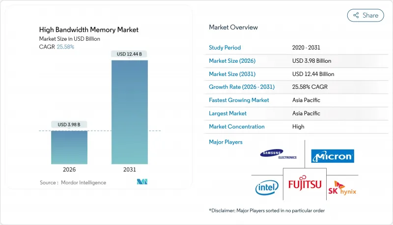
고대역폭 메모리 시장은 2025년 31억 7,000만 달러에서 2026년에는 39억 8,000만 달러로 성장하고 2026년부터 2031년에 걸쳐 CAGR 25.58%로 성장을 지속하여, 2031년까지 124억 4,000만 달러에 달할 것으로 예측됩니다.
2025년에는 AI 최적화 서버에 대한 지속적인 수요, DDR5의 보급 확대, 하이퍼스케일러에 의한 적극적인 투자가 더해져 반도체 밸류 체인 전체에서의 생산 능력 확대가 가속화되었습니다. 지난 1년간 공급업체는 TSV 수율 향상에 주력했지만, 패키징 파트너는 기판 부족을 완화하기 위해 새로운 CoWoS 라인에 대한 투자를 추진했습니다. 자동차 제조업체는 레벨 3 및 레벨 4 자율주행 플랫폼을 위한 ISO 26262 인증 획득 HBM을 확보하기 위해 메모리 공급업체와의 협력을 강화했습니다. 아시아태평양의 제조 에코시스템은 한국 업체들이 차세대 HBM4E 양산을 위한 수십억 달러 규모의 투자를 약속함으로써 생산면에서 주도권을 유지했습니다.
세계의 고대역폭 메모리 시장의 동향 및 인사이트
AI 서버의 보급과 GPU 연결률
거대 언어 모델의 급속한 성장으로 인해 2024년에는 기존 HPC 디바이스에 비해 GPU당 HBM 요구사항이 7배로 증가했습니다. NVIDIA의 H100은 80GB의 HBM3를 탑재해 3.35TB/s를 실현하는 한편 H200은 2025년 초에 141GB의 HBM3E를 탑재해 4.8TB/s를 실현하였습니다. 주문 잔여로 인해 2026년까지 공급업체의 생산 능력의 대부분이 확보될 전망이며 데이터센터 운영자는 재고 사전 구매 및 패키징 라인에 대한 공동 투자를 요구받고 있습니다.
데이터센터를 DDR5 및 2.5-D 패키징으로 마이그레이션
하이퍼스케일러 회사는 와트당 성능을 50% 향상시키기 위해 워크로드를 DDR4에서 DDR5로 마이그레이션하는 동시에 AI 가속기와 실리콘 인터포저의 적층 메모리를 연결하는 2.5-D 통합 기술을 채택했습니다. 기판 부족으로 인해 2024년 내내 GPU 출시가 지연되면서 단일 패키징 플랫폼에 대한 의존이 공급망 위험을 높였습니다.
12층 스택 초과 시 TSV 수율 저하
16층 HBM 스택에서는 열 사이클에 의한 TSV 내부의 구리 이동 고장이 발생하여 수율이 70%를 밑돌았습니다. 제조업체는 신뢰성 안정화를 위해, 열 대응 TSV 설계나 신규 유전체 재료를 추구하고 있지만 상용화에는 앞으로 2년이 소요될 전망입니다.
부문 분석
서버 카테고리는 2025년 고대역폭 메모리 시장에서 67.80%의 점유율을 차지했으며, 하이퍼스케일 사업자가 8-12개의 HBM 스택을 통합한 AI 서버로 이행한 점을 반영하여 시장을 견인했습니다. 클라우드 프로바이더가 GPU당 3TB/s 이상의 대역폭을 필요로 하는 기반 모델 서비스를 시작함으로써 수요가 가속화되었습니다. 2025년 에너지 효율 목표는 이산 솔루션보다 뛰어난 성능/와트를 제공하는 적층 DRAM이 우위를 차지하였으며 데이터센터 사업자의 전력 요건을 충족했습니다. 엔터프라이즈 리프레시 사이클이 시작되면서 DDR4 기반 노드를 HBM 지원 가속기로 대체하는 움직임이 2027년까지 구매 계약을 연장하고 있습니다.
자동차 및 운송부문은 현재 규모는 작지만, 2031년까지 연평균 복합 성장률(CAGR) 34.18%로 가장 높은 성장률을 나타낼 것으로 예측되고 있습니다. 칩 제조업체는 Tier 1 공급업체와 협력하여 ASIL D 요구사항을 충족하는 안전 기능을 통합했습니다. 유럽 및 북미의 레벨 3 생산 프로그램은 2024년 말에 제한적인 배포를 시작했으며 각 차량은 기존에 데이터센터 추론 클러스터 전용이었던 메모리 대역폭을 활용하고 있습니다. 무선 업데이트 전략이 성숙함에 따라 자동차 제조업체는 차량을 엣지 서버로 이용하고 이는 HBM 탑재율을 더욱 뒷받침합니다.
HBM3은 AI 트레이닝 GPU를 통해 보급이 확대되었으며, 2025년에는 매출의 45.70%를 차지했습니다. HBM3E 샘플 출하는 2024년 1분기에 시작되었으며, 1단계 생산에서는 9.2Gb/s 이상의 핀 속도로 가동되었습니다. 이후 성능 향상으로 스택당 1.2TB/s를 달성하여 목표 대역폭에 필요한 스택 수를 줄이고 패키지 열 밀도를 낮췄습니다.
HBM3E는 CAGR 40.90%을 나타낼 전망입니다. 이는 2025년 중반에 양산을 시작한 마이크론의 36GB 및 12 하이 제품에 의해 뒷받침되고 있으며, 최대 5,200억 파라미터의 모델 사이즈를 가지는 가속기를 대상으로 하고 있습니다. 향후 전망으로는, 2025년 4월에 공개된 HBM4 규격에서는 스택당 채널 수가 두배로 증가하여 총 처리량이 2TB/s로 향상되고 멀티페타플롭스급 AI 프로세서의 기반이 갖추어집니다.
고대역폭 메모리(HBM) 시장은 용도별(서버, 네트워크, 고성능 컴퓨팅, 소비자용 전자기기 등), 기술별(HBM2, HBM2E, HBM3, HBM3E, HBM4), 스택당 메모리 용량별(4GB, 8GB, 16GB, 24GB, 32GB 이상), 프로세서 인터페이스별(GPU, CPU, AI 가속기 및 ASIC, FPGA 등), 지역별(북미, 남미, 유럽, 아시아태평양, 중동, 아프리카)로 구분됩니다.
지역별 분석
아시아태평양은 2025년 매출의 41.00%를 차지하였으며 한국이 핵심을 담당하고 있습니다. 한국에서는 SK하이닉스와 삼성이 생산라인의 80% 이상을 지배하고 있습니다. 2024년에 발표된 정부 우대 조치는 2027년 가동 예정인 확장 제조 클러스터를 뒷받침하고 있습니다. 대만의 TSMC는 최첨단 CoWoS 패키징을 독점하고 있으나, 메모리 공급을 현지 기판 공급에 의존함으로써 지역적인 집중 위험을 초래하고 있습니다.
북미의 점유율은 마이크론사가 CHIPS법에 의해 61억 달러의 자금 조달을 확보하고, 뉴욕주와 아이다호주에 선진 DRAM 공장을 건설함으로써 증가했습니다. HBM의 파일럿 생산은 2026년 초 개시될 것으로 예상됩니다. 하이퍼스케일러의 설비투자가 현지 수요를 계속 견인하고 있지만, 대부분의 웨이퍼는 여전히 아시아에서 가공된 후 미국에서 최종 모듈 조립이 이루어지고 있습니다.
유럽은 자동차 수요를 기점으로 시장에 진입하고 있습니다. 독일의 자동차 제조업체는 2024년 말 출고된 레벨 3 운전 지원 시스템을 위한 HBM 인증을 완료했습니다. EU의 반도체 전략은 R&D 중심의 자세를 유지하면서 미래의 고대역폭 메모리 시장 확대의 핵심이 되는 포토닉 인터커넥트와 뉴로모픽 연구를 중시하고 있습니다. 중동 및 아프리카는 도입 초기 단계에 머무르고 있지만, 2025년에 시작된 국가 주도의 AI 데이터센터 프로젝트는 지역 수요의 증가를 시사합니다.
기타 혜택
- 시장 예측(ME) 엑셀 시트
- 3개월 애널리스트 서포트
자주 묻는 질문
목차
제1장 서론
- 조사의 전제조건 및 시장의 정의
- 조사 범위
제2장 조사 방법
제3장 주요 요약
제4장 시장 상황
- 시장 개요
- 촉진요인
- AI 서버의 보급과 GPU 탑재율 증가
- 데이터센터의 DDR5 및 2.5-D 패키징으로의 전환
- 자동차용 ADAS에서의 엣지 AI 추론
- 하이퍼스케일러에서 선호되는 실리콘 인터포저 스택
- 지역별 메모리 생산 보조금(한국, 미국, 일본)
- 포토닉스 대응 HBM 로드맵(HBM-P)
- 억제요인
- 12층 이상의 스택에서 발생하는 TSV 수율 손실
- 한정적인 CoWoS/SoIC 선진 패키징 능력
- 1TB/s 이상의 대역폭 디바이스에서 발생하는 열 스로틀링
- AI 가속기에 대한 지정학적 수출 규제
- 밸류체인 분석
- 규제 상황
- 기술 전망
- Porter's Five Forces 분석
- 공급자의 협상력
- 구매자의 협상력
- 신규 참가업체의 위협
- 대체품의 위협
- 경쟁 기업 간 경쟁 관계
- DRAM 시장 분석
- DRAM 수익과 예측
- 지역별 DRAM 수익
- DDR5 제품의 현행 가격
- DDR5 제품 제조업체 일람
- 거시경제 요인의 영향
제5장 시장 규모 및 성장 예측
- 용도별
- 서버
- 네트워크
- 고성능 컴퓨팅
- 소비자용 전자기기
- 자동차 및 운송 장비
- 기술별
- HBM2
- HBM2E
- HBM3
- HBM3E
- HBM4
- 메모리 용량별(스택당)
- 4GB
- 8GB
- 16GB
- 24GB
- 32GB 이상
- 프로세서 인터페이스별
- GPU
- CPU
- AI 가속기 및 ASIC
- FPGA
- 기타
- 지역별
- 북미
- 미국
- 캐나다
- 멕시코
- 남미
- 브라질
- 기타 남미
- 유럽
- 독일
- 프랑스
- 영국
- 기타 유럽
- 아시아태평양
- 중국
- 일본
- 인도
- 한국
- 기타 아시아태평양
- 중동 및 아프리카
- 중동
- 사우디아라비아
- 아랍에미리트(UAE)
- 튀르키예
- 기타 중동
- 아프리카
- 남아프리카
- 기타 아프리카
- 중동
- 북미
제6장 경쟁 구도
- 시장 집중도
- 전략적 동향
- 시장 점유율 분석
- 기업 프로파일
- Samsung Electronics Co., Ltd.
- SK hynix Inc.
- Micron Technology, Inc.
- Intel Corporation
- Advanced Micro Devices, Inc.
- Nvidia Corporation
- Taiwan Semiconductor Manufacturing Company Limited
- ASE Technology Holding Co., Ltd.
- Amkor Technology, Inc.
- Powertech Technology Inc.
- United Microelectronics Corporation
- GlobalFoundries Inc.
- Applied Materials Inc.
- Marvell Technology, Inc.
- Rambus Inc.
- Cadence Design Systems, Inc.
- Synopsys, Inc.
- Siliconware Precision Industries Co., Ltd.
- JCET Group Co., Ltd.
- Chipbond Technology Corporation
- Cadence Design Systems Inc.
- Broadcom Inc.
- Celestial AI
- ASE-SPIL(Silicon Products)
- Graphcore Limited
제7장 시장 기회 및 미래 전망
CSM 26.02.09The high bandwidth memory market is expected to grow from USD 3.17 billion in 2025 to USD 3.98 billion in 2026 and is forecast to reach USD 12.44 billion by 2031 at 25.58% CAGR over 2026-2031.

Sustained demand for AI-optimized servers, wider DDR5 adoption, and aggressive hyperscaler spending continued to accelerate capacity expansions across the semiconductor value chain in 2025. Over the past year, suppliers concentrated on TSV yield improvement, while packaging partners invested in new CoWoS lines to ease substrate shortages. Automakers deepened engagements with memory vendors to secure ISO 26262-qualified HBM for Level 3 and Level 4 autonomous platforms. Asia-Pacific's fabrication ecosystem retained production leadership after Korean manufacturers committed multibillion-dollar outlays aimed at next-generation HBM4E ramps.
Global High Bandwidth Memory Market Trends and Insights
AI-Server Proliferation and GPU Attach Rates
Rapid growth in large-scale language models drove a seven-fold rise in HBM per GPU requirements compared with traditional HPC devices during 2024. NVIDIA's H100 combined 80 GB of HBM3, delivering 3.35 TB/s, while the H200 was sampled in early 2025 with 141 GB of HBM3E at 4.8 TB/s. Order backlogs locked in the majority of supplier capacity through 2026, forcing data-center operators to pre-purchase inventory and co-invest in packaging lines.
Data-Center Shift to DDR5 and 2.5-D Packaging
Hyperscalers moved workloads from DDR4 to DDR5 to obtain 50% better performance per watt, simultaneously adopting 2.5-D integration that links AI accelerators to stacked memory on silicon interposers. Dependence on a single packaging platform heightened supply-chain risk when substrate shortages delayed GPU launches throughout 2024.
TSV Yield Losses Above 12-Layer Stacks
Yield fell below 70% on 16-high HBM stacks because thermal cycling induced copper-migration failures within TSVs. Manufacturers pursued thermal through-silicon via designs and novel dielectric materials to stabilize reliability, but commercialization remains two years away.
Other drivers and restraints analyzed in the detailed report include:
- Edge-AI Inference in Automotive ADAS
- Hyperscaler Preference for Silicon Interposer Stacks
- Limited CoWoS/SoIC Advanced-Packaging Capacity
For complete list of drivers and restraints, kindly check the Table Of Contents.
Segment Analysis
The server category led the high bandwidth memory market with a 67.80% revenue share in 2025, reflecting hyperscale operators' pivot to AI servers that each integrate eight to twelve HBM stacks. Demand accelerated after cloud providers launched foundation-model services that rely on per-GPU bandwidth above 3 TB/s. Energy efficiency targets in 2025 favored stacked DRAM because it delivered superior performance-per-watt over discrete solutions, enabling data-center operators to stay within power envelopes. An enterprise refresh cycle began as companies replaced DDR4-based nodes with HBM-enabled accelerators, extending purchasing commitments into 2027.
The automotive and transportation segment, while smaller today, recorded the fastest growth with a projected 34.18% CAGR through 2031. Chipmakers collaborated with Tier 1 suppliers to embed functional-safety features that meet ASIL D requirements. Level 3 production programs in Europe and North America entered limited rollout in late 2024, each vehicle using memory bandwidth previously reserved for data-center inference clusters. As over-the-air update strategies matured, vehicle manufacturers began treating cars as edge servers, further sustaining HBM attach rates.
HBM3 accounted for 45.70% revenue in 2025 after widespread adoption in AI training GPUs. Sampling of HBM3E started in Q1 2024, and first-wave production ran at pin speeds above 9.2 Gb/s. Performance gains reached 1.2 TB/s per stack, reducing the number of stacks needed for the target bandwidth and lowering package thermal density.
HBM3E's 40.90% forecast CAGR is underpinned by Micron's 36 GB, 12-high product that entered volume production in mid-2025, targeting accelerators with model sizes up to 520 billion parameters. Looking forward, the HBM4 standard published in April 2025 doubles channels per stack and raises aggregate throughput to 2 TB/s, setting the stage for multi-petaflop AI processors.
High Bandwidth Memory (HBM) Market is Segmented by Application (Servers, Networking, High-Performance Computing, Consumer Electronics, and More), Technology (HBM2, HBM2E, HBM3, HBM3E, and HBM4), Memory Capacity Per Stack (4 GB, 8 GB, 16 GB, 24 GB, and 32 GB and Above), Processor Interface (GPU, CPU, AI Accelerator/ASIC, FPGA, and More), and Geography (North America, South America, Europe, Asia-Pacific, and Middle East and Africa).
Geography Analysis
Asia-Pacific accounted for 41.00% of 2025 revenue, anchored by South Korea, where SK Hynix and Samsung controlled more than 80% of production lines. Government incentives announced in 2024 supported an expanded fabrication cluster scheduled to open in 2027. Taiwan's TSMC maintained a packaging monopoly for leading-edge CoWoS, tying memory availability to local substrate supply and creating a regional concentration risk.
North America's share grew as Micron secured USD 6.1 billion in CHIPS Act funding to build advanced DRAM fabs in New York and Idaho, with pilot HBM runs expected in early 2026. Hyperscaler capital expenditures continued to drive local demand, although most wafers were still processed in Asia before final module assembly in the United States.
Europe entered the market through automotive demand; German OEMs qualified HBM for Level 3 driver-assist systems shipping in late 2024. The EU's semiconductor strategy remained R&D-centric, favoring photonic interconnect and neuromorphic research that could unlock future high bandwidth memory market expansion. Middle East and Africa stayed in an early adoption phase, yet sovereign AI datacenter projects initiated in 2025 suggested a coming uptick in regional demand.
- Samsung Electronics Co., Ltd.
- SK hynix Inc.
- Micron Technology, Inc.
- Intel Corporation
- Advanced Micro Devices, Inc.
- Nvidia Corporation
- Taiwan Semiconductor Manufacturing Company Limited
- ASE Technology Holding Co., Ltd.
- Amkor Technology, Inc.
- Powertech Technology Inc.
- United Microelectronics Corporation
- GlobalFoundries Inc.
- Applied Materials Inc.
- Marvell Technology, Inc.
- Rambus Inc.
- Cadence Design Systems, Inc.
- Synopsys, Inc.
- Siliconware Precision Industries Co., Ltd.
- JCET Group Co., Ltd.
- Chipbond Technology Corporation
- Cadence Design Systems Inc.
- Broadcom Inc.
- Celestial AI
- ASE-SPIL (Silicon Products)
- Graphcore Limited
Additional Benefits:
- The market estimate (ME) sheet in Excel format
- 3 months of analyst support
TABLE OF CONTENTS
1 INTRODUCTION
- 1.1 Study Assumptions and Market Definition
- 1.2 Scope of the Study
2 RESEARCH METHODOLOGY
3 EXECUTIVE SUMMARY
4 MARKET LANDSCAPE
- 4.1 Market Overview
- 4.2 Market Drivers
- 4.2.1 AI-server proliferation and GPU attach rates
- 4.2.2 Data-center shift to DDR5 and 2.5-D packaging
- 4.2.3 Edge-AI inference in automotive ADAS
- 4.2.4 Hyperscaler preference for silicon interposer stacks
- 4.2.5 Localized memory production subsidies (KR, US, JP)
- 4.2.6 Photonics-ready HBM road-maps (HBM-P)
- 4.3 Market Restraints
- 4.3.1 TSV yield losses above 12-layer stacks
- 4.3.2 Limited CoWoS/SoIC advanced-packaging capacity
- 4.3.3 Thermal throttling in >1 TB/s bandwidth devices
- 4.3.4 Geo-political export controls on AI accelerators
- 4.4 Value Chain Analysis
- 4.5 Regulatory Landscape
- 4.6 Technological Outlook
- 4.7 Porter's Five Forces Analysis
- 4.7.1 Bargaining Power of Suppliers
- 4.7.2 Bargaining Power of Buyers
- 4.7.3 Threat of New Entrants
- 4.7.4 Threat of Substitutes
- 4.7.5 Intensity of Competitive Rivalry
- 4.8 DRAM Market Analysis
- 4.8.1 DRAM Revenue and Demand Forecast
- 4.8.2 DRAM Revenue by Geography
- 4.8.3 Current Pricing of DDR5 Products
- 4.8.4 List of DDR5 Product Manufacturers
- 4.9 Impact of Macroeconomic Factors
5 MARKET SIZE AND GROWTH FORECASTS (VALUE)
- 5.1 By Application
- 5.1.1 Servers
- 5.1.2 Networking
- 5.1.3 High-Performance Computing
- 5.1.4 Consumer Electronics
- 5.1.5 Automotive and Transportation
- 5.2 By Technology
- 5.2.1 HBM2
- 5.2.2 HBM2E
- 5.2.3 HBM3
- 5.2.4 HBM3E
- 5.2.5 HBM4
- 5.3 By Memory Capacity per Stack
- 5.3.1 4 GB
- 5.3.2 8 GB
- 5.3.3 16 GB
- 5.3.4 24 GB
- 5.3.5 32 GB and Above
- 5.4 By Processor Interface
- 5.4.1 GPU
- 5.4.2 CPU
- 5.4.3 AI Accelerator / ASIC
- 5.4.4 FPGA
- 5.4.5 Others
- 5.5 By Geography
- 5.5.1 North America
- 5.5.1.1 United States
- 5.5.1.2 Canada
- 5.5.1.3 Mexico
- 5.5.2 South America
- 5.5.2.1 Brazil
- 5.5.2.2 Rest of South America
- 5.5.3 Europe
- 5.5.3.1 Germany
- 5.5.3.2 France
- 5.5.3.3 United Kingdom
- 5.5.3.4 Rest of Europe
- 5.5.4 Asia-Pacific
- 5.5.4.1 China
- 5.5.4.2 Japan
- 5.5.4.3 India
- 5.5.4.4 South Korea
- 5.5.4.5 Rest of Asia-Pacific
- 5.5.5 Middle East and Africa
- 5.5.5.1 Middle East
- 5.5.5.1.1 Saudi Arabia
- 5.5.5.1.2 United Arab Emirates
- 5.5.5.1.3 Turkey
- 5.5.5.1.4 Rest of Middle East
- 5.5.5.2 Africa
- 5.5.5.2.1 South Africa
- 5.5.5.2.2 Rest of Africa
- 5.5.5.1 Middle East
- 5.5.1 North America
6 COMPETITIVE LANDSCAPE
- 6.1 Market Concentration
- 6.2 Strategic Moves
- 6.3 Market Share Analysis
- 6.4 Company Profiles (includes Global-level Overview, Market-level Overview, Core Segments, Financials, Strategic Information, Market Rank/Share, Products and Services, Recent Developments)
- 6.4.1 Samsung Electronics Co., Ltd.
- 6.4.2 SK hynix Inc.
- 6.4.3 Micron Technology, Inc.
- 6.4.4 Intel Corporation
- 6.4.5 Advanced Micro Devices, Inc.
- 6.4.6 Nvidia Corporation
- 6.4.7 Taiwan Semiconductor Manufacturing Company Limited
- 6.4.8 ASE Technology Holding Co., Ltd.
- 6.4.9 Amkor Technology, Inc.
- 6.4.10 Powertech Technology Inc.
- 6.4.11 United Microelectronics Corporation
- 6.4.12 GlobalFoundries Inc.
- 6.4.13 Applied Materials Inc.
- 6.4.14 Marvell Technology, Inc.
- 6.4.15 Rambus Inc.
- 6.4.16 Cadence Design Systems, Inc.
- 6.4.17 Synopsys, Inc.
- 6.4.18 Siliconware Precision Industries Co., Ltd.
- 6.4.19 JCET Group Co., Ltd.
- 6.4.20 Chipbond Technology Corporation
- 6.4.21 Cadence Design Systems Inc.
- 6.4.22 Broadcom Inc.
- 6.4.23 Celestial AI
- 6.4.24 ASE-SPIL (Silicon Products)
- 6.4.25 Graphcore Limited
7 MARKET OPPORTUNITIES AND FUTURE OUTLOOK
- 7.1 White-space and Unmet-need Assessment
