
|
시장보고서
상품코드
2035030
웨이퍼 프로버 시장 : 점유율 분석, 업계 동향 및 통계, 성장 예측(2026-2031년)Wafer Prober - Market Share Analysis, Industry Trends & Statistics, Growth Forecasts (2026 - 2031) |
||||||
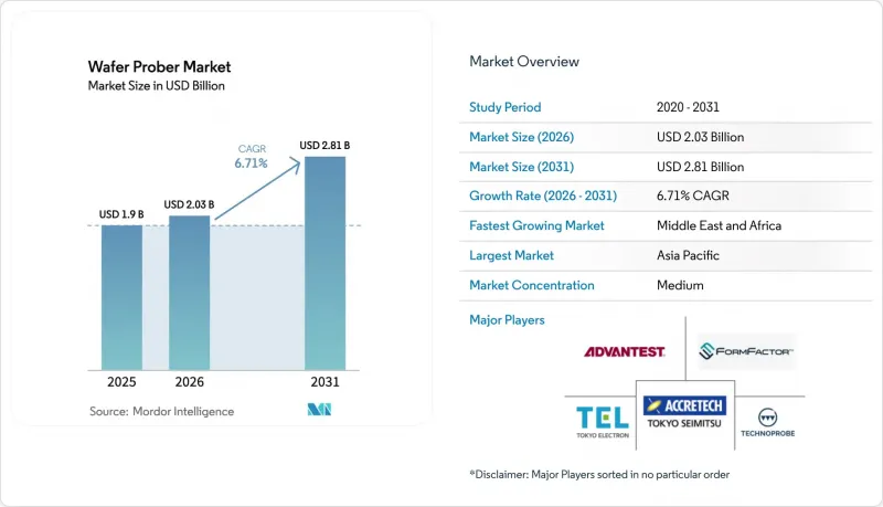
2026년 웨이퍼 프로버 시장 규모는 20억 3,000만 달러로 추정되며 2025년 19억 달러에서 확대해, 2031년에는 28억 1,000만 달러에 이를 것으로 예측됩니다.
2026년부터 2031년까지 연평균 복합 성장률(CAGR) 6.71%를 나타낼 것으로 예측됩니다.
이러한 견조한 성장은 반도체 부문의 생산 능력 확대와 패키징 전에 점점 더 소형화, 고성능화되는 칩에 대한 검증의 필요성에 직접적으로 기인하고 있습니다. 첨단 패키징 기술의 대량 도입, AI 및 5G 디바이스 생산의 급증, 그리고 더 큰 웨이퍼 포맷으로의 전환은 차세대 웨이퍼 프로버에 대한 수요를 촉진하고 있습니다. 각 벤더들은 AI를 고장 감지에 접목하고, 예지보전을 통합하고, 프로브 카드의 정확도를 향상시켜 테스트 비용을 낮추면서 처리량을 증가시킴으로써 이러한 수요에 대응하고 있습니다. 2024년에는 완전 자동 부문이 웨이퍼 프로버 시장의 64.1%를 차지하며 1위를 차지했습니다. 이는 무인화 제조(Lights-out Manufacturing)를 지향하는 공장 전체 자동화 프로그램에 의해 뒷받침된 것입니다. 접촉식 프로버는 여전히 87.2%의 점유율을 차지하며 일상적인 테스트 현장을 지배하고 있지만, 비접촉식 RF 솔루션은 Sub-THz 디바이스를 지원하기 위해 빠르게 성장하고 있습니다.
세계 웨이퍼 프로버 시장 동향 및 인사이트
3D IC 및 첨단 패키징의 급성장
테스트 요구사항이 재정의되고 있는 가운데, 칩렛 아키텍처와 이기종 통합이 광범위하게 채택되고 있습니다. 멀티 다이 스태킹의 도입으로 고밀도 수직 상호연결 및 새로운 신뢰성 체크포인트가 생겨났지만, 기존의 웨이퍼 프로버 설계로는 이러한 문제를 완전히 해결할 수 없습니다. 프로브 카드 공급업체들은 현재 방대한 인터포저 표면을 커버하기 위해 터치다운 당 수천 개의 접점 수를 가진 고핀 수 MEMS 어레이를 도입하고 있습니다. FormFactor의 고급 패키지용 커스텀 카드는 여러 개의 다이를 동시에 테스트하여 신호 무결성을 보장하면서 테스트 시간을 단축할 수 있는 방법을 제시합니다. 따라서 웨이퍼 프로버 시장은 ±50mK의 안정성을 갖춘 고밀도, 열 제어식 플래튼으로 전환하고 있으며, 전력 소모가 큰 AI 가속기에 대한 일관된 측정을 보장하고 있습니다.
AI/5G 디바이스 생산량 급증
AI 프로세서와 5G 칩셋의 폭발적인 증가로 팹은 마진을 희생하지 않고 시간당 디바이스 테스트 횟수를 크게 늘려야 합니다. 최신 AI SoC는 프로브 패드를 다이의 가장자리까지 밀고 50µm의 피치 균일성을 요구하는 고대역폭 메모리 스택을 통합하고 있습니다. 웨이퍼 한 장당 2초 이내에 정렬을 자가 교정하는 전자동 프로버는 현재 양산 라인의 중심이 되고 있습니다. "Semiconductor Engineering 저널은 AI 중심 테스트는 프로브 카드, 핸들러, ATE의 각 레벨에서 병렬 처리가 필요하며, 이러한 패러다임은 전류 소비와 데이터 로깅의 복잡성을 증가시킨다고 지적합니다. 각 공급업체들은 머신러닝 기반의 스케줄링을 도입하여 가장 혼잡하지 않은 프로버에 웨이퍼를 배치함으로써 장비의 총효율(OEE)을 극대화하고 있습니다.
고가의 설비 투자 및 긴 회수 기간
차세대 전자동 프로버는 대당 300만 달러가 넘는 경우가 많아 중소형 팹의 현금 흐름에 부담을 주고 있습니다. 노드의 복잡성에 따라 프로브카드와 데이터 분석 플랫폼에 대한 병행 투자가 요구되면서 설비 감가상각 기간이 길어지고 있습니다. EPD Tech의 추정에 따르면, 7nm 이하의 제조 비용은 10억 달러 이상이며, 투자 회수 기간(ROI)은 24개월 이상에 달할 전망입니다. 따라서 웨이퍼 프로버 시장에서는 구매를 미루거나 테스트한 웨이퍼 수에 따라 지불하는 리스 모델을 채택하여 설비투자(Cap-ex)를 운영비(Op-ex)로 전환하는 움직임이 나타나고 있습니다.
부문 분석
2025년 기준, 전자동 클래스는 웨이퍼 프로버 시장 점유율의 63.52%를 차지하며 CAGR 8.91%를 나타낼 것으로 예측됐습니다. 각 벤더들은 로봇식 웨이퍼 로더, 비전 가이드를 통한 정렬, 팹의 MES 시스템과 원활하게 연동되는 SECS/GEM 인터페이스를 통합하고 있습니다. SEMICON China의 제품 혁신상을 수상한 SEMISHARE A12 스테이션은 WAT, CP, RF 스윕 전체에서 1µm 미만의 스텝 사이즈 정확도를 실현했습니다. 한국이나 대만의 팹에서는 24시간 풀가동으로 운영되고 있으며, 가동률은 90%를 상회하고 있습니다.
반자동 유닛은 사이클 타임의 중요도는 낮지만, 유연성이 중시되는 중-대량 생산 제품 라인에서 여전히 일정한 지위를 유지하고 있습니다. 수동 프로브는 출하 수량이 적고 패드에 대한 빠른 접근이 자동 웨이퍼 교환 속도보다 우선시되는 대학 실험실 및 초기 디바이스 특성 평가에서 여전히 표준으로 사용되고 있습니다.
접촉식 프로빙은 성숙한 프로브 카드 생태계와 검증된 전기적 성능 덕분에 2025년 매출의 86.55%를 차지했습니다. 그러나 비접촉식 방식은 CAGR 13.56%를 기록하며 현재 가장 주목받는 연구개발의 초점이 되고 있습니다. IEEE Transactions에 실린 연구에서는 물리적 핀을 사용하지 않고 0Hz-340GHz의 연속 커버리지를 구현하는 유전체 도파관 커플러를 소개했습니다. 무선 RF 시스템은 프로브 마크의 손상을 방지하고 재프로빙 주기를 늘릴 수 있으며, 이는 취약한 화합물 반도체 웨이퍼에 큰 이점이 될 수 있습니다.
웨이퍼 프로버 시장에서는 100GHz를 넘어서는 6G 프로토타입이 등장하면서 한 번의 터치다운으로 DC 파라메트릭 측정과 원거리 방사 스윕을 수행하는 파일럿 셀이 등장하고 있습니다.
지역별 분석
아시아태평양은 대만, 한국, 중국 본토의 밀집된 팹 클러스터에 힘입어 2025년 웨이퍼 프로버 시장 규모의 47.05%를 차지했습니다. TSMC의 경우, 2024년 4분기 매출의 74%를 7nm 및 그보다 미세한 공정 노드가 차지하며, 최첨단 노드로의 지역적 경향을 뒷받침하고 있습니다. 각 지역 정부는 세제 혜택과 전력 보조금을 도입하여 생산 능력을 더욱 확대하기 위해 노력하고 있으며, 국내 프로브카드 업체들은 공급 리드 타임을 단축하기 위해 노력하고 있습니다.
중동 및 아프리카는 CAGR 11.24%로 가장 빠른 성장세를 보이고 있으며, 사우디아라비아의 1,000억 달러 규모의 'Alat' 이니셔티브는 2030년까지 최소 50개 이상의 설계 회사를 유치하는 것을 목표로 하고 있습니다. UAE는 자유무역지대 특혜를 배경으로 기업 유치가 진행되고 있으며, TSMC가 애리조나주 모델을 본뜬 UAE에 거점 설치를 검토하고 있다는 보도도 있습니다. AI 및 국방용 칩에 대한 현지 수요로 인해, 200mm 스타트업 라인에 최적화된 중형 프로버를 갖춘 새로운 연구소를 설립하게 되었습니다.
북미는 527억 달러 규모의 'CHIPS법'과 300mm 공정에 특화된 R&D 센터 계획의 혜택을 받고 있습니다. 애리조나 주립대학교 연구단지에는 프론트엔드 제조 및 첨단 패키징을 위한 플래그십 테스트베드가 설치될 예정입니다. 유럽은 '유럽칩법'을 통해 자율성을 추구하고 있으며, 독일, 프랑스, 아일랜드의 프로버 설비 현대화를 위한 보조금을 배분하고 있습니다. 이러한 노력은 전반적으로 아시아 수입 의존도를 낮추고 웨이퍼 프로버 시장의 수익 기반을 다변화하는 것을 목표로 하고 있습니다.
기타 특전:
- 엑셀 형식 시장 예측(ME) 시트
- 3개월간 애널리스트 지원
자주 묻는 질문
목차
제1장 서론
제2장 조사 방법
제3장 주요 요약
제4장 시장 구도
제5장 시장 규모와 성장 예측
제6장 경쟁 구도
제7장 시장 기회와 향후 전망
JHS 26.05.20The wafer prober market size in 2026 is estimated at USD 2.03 billion, growing from 2025 value of USD 1.90 billion with 2031 projections showing USD 2.81 billion, growing at 6.71% CAGR over 2026-2031.

This solid growth links directly to the semiconductor sector's rising production capacity and the need to validate ever-smaller, higher-performance chips before packaging. High-volume adoption of advanced packaging, the surge in AI and 5G device output, and the transition to larger wafer formats each reinforce demand for next-generation wafer probers. Vendors are responding by embedding AI in fault detection, integrating predictive maintenance, and improving probe-card precision to keep throughput high and test costs low. The fully automatic segment leads with a 64.1% wafer prober market share in 2024, aided by factory-wide automation programs that target lights-out manufacturing. Contact-based probers still dominate day-to-day test floors, holding 87.2% share, yet non-contact RF solutions are scaling fast to support sub-THz devices.
Global Wafer Prober Market Trends and Insights
3-D IC and Advanced Packaging Boom
Widespread adoption of chiplet architectures and heterogeneous integration is reshaping test requirements. Multidie stacking introduces dense vertical interconnects and new reliability checkpoints that traditional wafer prober designs cannot wholly address. Probe-card suppliers now deploy high-pin-count MEMS arrays that reach thousands of contacts per touchdown to cover large interposer surfaces. FormFactor's custom cards for advanced packages illustrate how simultaneous testing of multiple dies cuts test time while safeguarding signal integrity. The wafer prober market is thus pivoting to high-density, thermally controlled platens capable of +- 50 mK stability, ensuring consistent measurements for power-hungry AI accelerators.
AI / 5G Device Volume Upswing
The explosion of AI processors and 5G chipsets pressures fabs to test far more devices per hour without sacrificing margin. Modern AI SOCs integrate high-bandwidth memory stacks that push probe pads to the edge of the die and demand 50 µm pitch uniformity. Fully automatic probers that self-calibrate alignment in under 2 s per wafer are now central to mass-production lines. Semiconductor Engineering notes that AI-centric testing requires parallelism at the probe card, handler, and ATE levels, a paradigm that raises both current draw and data-logging complexity. Suppliers are adding machine-learning-based scheduling to route wafers to the least congested probers, maximizing overall equipment effectiveness.
High Cap-ex and Long Pay-back
Next-generation fully automatic probers routinely cross USD 3 million per unit, straining cash flow among smaller fabs. Equipment depreciation timelines have stretched as node complexity forces parallel investments in probe cards and data-analytic platforms. EPD Tech calculates that sub-7 nm production costs have topped USD 1 billion, extending ROI horizons beyond 24 months. The wafer prober market thus witnesses deferred purchases or lease models where manufacturers pay by the tested wafer, shifting cap-ex to op-ex.
Other drivers and restraints analyzed in the detailed report include:
- Migration to 200- and 300 mm Fabs
- SiC / GaN Power-Device Ramp-up
- Rising Test-Time per Advanced Node
For complete list of drivers and restraints, kindly check the Table Of Contents.
Segment Analysis
The fully automatic class held a commanding 63.52% wafer prober market share in 2025 and is forecast to post a 8.91% CAGR. Vendors embed robotic wafer loaders, vision-guided alignment, and SECS/GEM interfaces that connect seamlessly with fab MES systems. The SEMISHARE A12 station, recipient of SEMICON China's product innovation award, illustrates step-size accuracy below 1 µm across WAT, CP, and RF sweeps. Labor-light fabs in Korea and Taiwan schedule fleet operation around the clock, lifting utilization rates above 90%.
Semi-automatic units retain a foothold in mid-volume product lines where cycle time is less critical, but flexibility is prized. Manual probes, though small in shipment volume, remain staples in university labs and early device characterization, where quick pad access outweighs automatic wafer exchange speeds.
Contact-based probing still captured 86.55% of 2025 revenue thanks to mature probe-card ecosystems and proven electrical performance. Yet non-contact methods posted a 13.56% CAGR and are now the hottest R&D focus. An IEEE Transactions study described dielectric waveguide couplers that deliver continuous 0 Hz-340 GHz coverage without physical pins. RF-over-air systems avoid probe-mark damage and enable higher reprobing cycles, a major plus for fragile compound-semiconductor wafers.
Probe-card leaders respond with hybrid offerings: vertical MEMS springs for power rails and contactless couplers for millimeter-wave nets on the same card. As 6G prototypes move above 100 GHz, the wafer prober market sees pilot cells that perform DC parametrics and far-field radiation sweeps in a single touchdown.
Wafer Prober Market is Segmented by Product Type (Manual, Semi-Automatic, and Fully Automatic), Technology (Contact, and Non-Contact), Application (Wafer Sort / CP, Package-Level Final Test, and R&D / Failure Analysis), Wafer Size (<=150 Mm, 150-200 Mm, 200-300 Mm, and More), End-User (Foundries, Idms, Osats, and Research and Academia), and Geography (North America, South America, Europe, Asia-Pacific, and Middle East and Africa).
Geography Analysis
Asia-Pacific held 47.05% of the wafer prober market size in 2025, powered by the dense fab clusters of Taiwan, South Korea, and mainland China. TSMC alone reported 74% of Q4 2024 revenue from 7 nm and finer geometries, reinforcing the regional tilt toward cutting-edge nodes. Regional governments offer tax holidays and electricity subsidies that encourage further capacity builds, while domestic probe-card vendors shorten supply lead times.
The Middle East and Africa show the fastest trajectory at an 11.24% CAGR, with Saudi Arabia's USD 100 billion Alat initiative targeting at least 50 design houses by 2030. The UAE courts are founded with free-zone incentives, and reports suggest TSMC is evaluating a UAE site that mirrors its Arizona model. Local demand for AI and defense chips translates into greenfield labs equipped with mid-range probers optimized for 200 mm startup lines.
North America benefits from the USD 52.7 billion CHIPS Act and a pipeline of 300 mm-focused R&D centers. The Arizona State University Research Park will host a flagship testbed for front-end manufacturing and advanced packaging. Europe pursues autonomy via the European Chips Act, allocating grants that modernize probe capacity in Germany, France, and Ireland. Collectively, these initiatives aim to curb reliance on Asian imports and diversify the wafer prober market's revenue base.
- Tokyo Electron Ltd
- Advantest Corp
- FormFactor Inc
- SemiShare Co Ltd
- Micronics Japan Co Ltd
- Accretech (Tokyo Seimitsu)
- MPI Corp
- Wentworth Laboratories Inc
- Technoprobe S.p.A.
- TSE Co Ltd
- Semics Inc
- EverBeing Int'l Corp
- Signatone Corp
- MicroXact Inc
- SEMICAPS Pte Ltd
- Feinmetall GmbH
- INGUN Prufmittelbau GmbH
- SV Probe Pte Ltd
- Chunghwa Precision Test Tech
- Suragus GmbH
- Wuxi Junr Technology Co., Ltd. (JUNR)
- China Micro Semicon Equip (CSEM)
- Signatone Corp
- Tipronics Co Ltd
- STAr Technologies Inc.
- Shibasoku Co Ltd
Additional Benefits:
- The market estimate (ME) sheet in Excel format
- 3 months of analyst support
TABLE OF CONTENTS
1 INTRODUCTION
- 1.1 Study Assumptions and Market Definition
- 1.2 Scope of the Study
2 RESEARCH METHODOLOGY
3 EXECUTIVE SUMMARY
4 MARKET LANDSCAPE
- 4.1 Market Overview
- 4.2 Market Drivers
- 4.2.1 3-D IC and Advanced Packaging Boom
- 4.2.2 AI / 5 G Device Volume Upswing
- 4.2.3 Migration to 200- and 300-mm Fabs
- 4.2.4 SiC / GaN Power-Device Ramp-up
- 4.2.5 National Chip-Fab Subsidies (US/EU)
- 4.2.6 MEMS Micro-probe Array Adoption
- 4.3 Market Restraints
- 4.3.1 High Cap-ex and Long Pay-back
- 4.3.2 Rising Test-time per Advanced Node
- 4.3.3 Precision Probe-Card Supply Bottlenecks
- 4.3.4 In-situ Litho-Stage Test Alternatives
- 4.4 Value Chain Analysis
- 4.5 Regulatory Landscape
- 4.6 Technological Outlook
- 4.7 Porter's Five Forces Analysis
- 4.7.1 Bargaining Power of Suppliers
- 4.7.2 Bargaining Power of Buyers
- 4.7.3 Threat of New Entrants
- 4.7.4 Threat of Substitutes
- 4.7.5 Competitive Rivalry
- 4.8 Impact of Macroeconomic Factors
5 MARKET SIZE AND GROWTH FORECASTS (VALUE)
- 5.1 By Product Type
- 5.1.1 Manual
- 5.1.2 Semi-Automatic
- 5.1.3 Fully Automatic
- 5.2 By Technology
- 5.2.1 Contact
- 5.2.2 Non-contact / RF-over-Air
- 5.3 By Application
- 5.3.1 Wafer Sort / CP
- 5.3.2 Package-Level Final Test
- 5.3.3 R&D / Failure Analysis
- 5.4 By Wafer Size
- 5.4.1 <=150 mm
- 5.4.2 150-200 mm
- 5.4.3 200-300 mm
- 5.4.4 >300 mm (450 mm, Panel)
- 5.5 By End-user
- 5.5.1 Foundries
- 5.5.2 IDMs
- 5.5.3 OSATs
- 5.5.4 Research and Academia
- 5.6 By Geography
- 5.6.1 North America
- 5.6.1.1 United States
- 5.6.1.2 Canada
- 5.6.1.3 Mexico
- 5.6.2 South America
- 5.6.2.1 Brazil
- 5.6.2.2 Argentina
- 5.6.2.3 Rest of South America
- 5.6.3 Europe
- 5.6.3.1 Germany
- 5.6.3.2 United Kingdom
- 5.6.3.3 France
- 5.6.3.4 Italy
- 5.6.3.5 Spain
- 5.6.3.6 Russia
- 5.6.3.7 Rest of Europe
- 5.6.4 Asia-Pacific
- 5.6.4.1 China
- 5.6.4.2 Japan
- 5.6.4.3 India
- 5.6.4.4 South Korea
- 5.6.4.5 South-East Asia
- 5.6.4.6 Rest of Asia-Pacific
- 5.6.5 Middle East and Africa
- 5.6.5.1 Middle East
- 5.6.5.1.1 Saudi Arabia
- 5.6.5.1.2 United Arab Emirates
- 5.6.5.1.3 Turkey
- 5.6.5.1.4 Rest of Middle East
- 5.6.5.2 Africa
- 5.6.5.2.1 South Africa
- 5.6.5.2.2 Nigeria
- 5.6.5.2.3 Rest of Africa
- 5.6.5.1 Middle East
- 5.6.1 North America
6 COMPETITIVE LANDSCAPE
- 6.1 Market Concentration
- 6.2 Strategic Moves
- 6.3 Market Share Analysis
- 6.4 Company Profiles (includes Global-level Overview, Market-level Overview, Core Segments, Financials, Strategic Info, Market Rank/Share, Products and Services, Recent Developments)
- 6.4.1 Tokyo Electron Ltd
- 6.4.2 Advantest Corp
- 6.4.3 FormFactor Inc
- 6.4.4 SemiShare Co Ltd
- 6.4.5 Micronics Japan Co Ltd
- 6.4.6 Accretech (Tokyo Seimitsu)
- 6.4.7 MPI Corp
- 6.4.8 Wentworth Laboratories Inc
- 6.4.9 Technoprobe S.p.A.
- 6.4.10 TSE Co Ltd
- 6.4.11 Semics Inc
- 6.4.12 EverBeing Int'l Corp
- 6.4.13 Signatone Corp
- 6.4.14 MicroXact Inc
- 6.4.15 SEMICAPS Pte Ltd
- 6.4.16 Feinmetall GmbH
- 6.4.17 INGUN Prufmittelbau GmbH
- 6.4.18 SV Probe Pte Ltd
- 6.4.19 Chunghwa Precision Test Tech
- 6.4.20 Suragus GmbH
- 6.4.21 Wuxi Junr Technology Co., Ltd. (JUNR)
- 6.4.22 China Micro Semicon Equip (CSEM)
- 6.4.23 Signatone Corp
- 6.4.24 Tipronics Co Ltd
- 6.4.25 STAr Technologies Inc.
- 6.4.26 Shibasoku Co Ltd
7 MARKET OPPORTUNITIES AND FUTURE OUTLOOK
- 7.1 White-space and Unmet-need Assessment
