
|
시장보고서
상품코드
2065509
인공지능(AI) 가속기용 2.5D 및 3D IC 패키징 : 시장 점유율 분석, 업계 동향 및 통계, 성장 예측(2026-2031년)2.5D And 3D IC Packaging For AI Accelerators - Market Share Analysis, Industry Trends & Statistics, Growth Forecasts (2026 - 2031) |
||||||
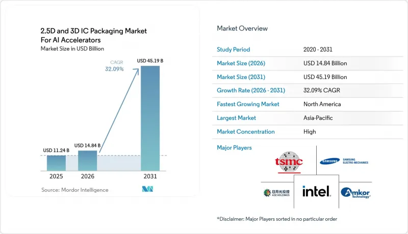
인공지능(AI) 가속기용 2.5D 및 3D IC 패키징 시장 규모는 2026년 148억 4,000만 달러에서 2031년까지 451억 9,000만 달러로 확대되어 2026년부터 2031년에 걸쳐 CAGR 32.09%를 나타낼 것으로 예측되고 있습니다.

본 보고서는 패키징 기술(2.5D IC 패키징 등), 패키징 플랫폼(CoWoS, I-Cube, Foveros, EMIB 등), 용도(AI 훈련 가속기, AI 추론 가속기 등), 최종 사용자(하이퍼스케일러 및 클라우드 제공업체, 엔터프라이즈 AI 인프라 등), 그리고 지역별로 분류되어 있습니다. 시장 전망은 금액(달러) 기준으로 제시되어 있습니다.
인공지능(AI) 가속기용 2.5D 및 3D IC 패키징 시장에 대한 동향 및 인사이트
파운데이션 모델에서 훈련 연산 요구량의 폭발적인 증가
현재 훈련 실행 횟수는 1,025회의 부동소수점 연산을 넘어, 2020년 벤치마크의 100배에 달하고 있습니다. OpenAI는 GPT-4개발에 2만 5,000대의 NVIDIA A100 GPU가 필요했으며, 메타의 4,050억 파라미터를 가진 Llama 3.1은 1만 6,000대 이상의 H100S를 소모했습니다. 이러한 클러스터에서는 텐서 코어가 최대 가동 상태에 도달하기도 전에 HBM3E의 대역폭이 포화 상태에 이르기 때문에 아키텍트들은 다이 간 대역폭 10 TB/s를 제공하는 CoWoS-L과 같은 2.5D 인터포저를 채택할 수밖에 없습니다. 또한, 듀얼 다이 GPU를 통해 공급업체는 수율이 낮은 타일을 효율적으로 활용할 수 있어 웨이퍼 전체의 경제성을 높일 수 있습니다. 연구자들이 2027년까지 10조 파라미터 규모의 모델을 목표로 하고 있는 가운데, 대역폭과 전력 공급 수요를 충족시키기 위한 주요 수단으로서 패키징의 중요성은 앞으로도 변함없을 것입니다.
클라우드 데이터센터에서 AI 가속기의 급속한 업데이트 주기
각 하이퍼스케일러 기업들은 가속기의 교체 주기를 2년에서 1년으로 단축하고 있습니다. 마이크로소프트는 2025년 하반기에 Azure 전체에 Maia 200을 배포할 예정이며, 구글은 2025년에 TPU v8의 양산 출하를 시작했고, AWS는 2024년에 Trainium 2를 도입했습니다. 각 SKU에는 로직, 메모리, 아날로그 I/O 다이를 단일 실적에 통합한 패키징이 필요합니다. 지연 시간에 민감한 추론용 변형에서는 수직 적층 방식이 점점 더 선호되고 있어, 공급업체들은 하이브리드 본딩으로의 전환을 서둘러야 하는 상황에 처해 있습니다. CoWoS 라인의 리드타임은 6-9개월이므로, 생산 할당량을 확보하기 위해서는 파운드리와의 장기적인 제휴가 결정적인 요소가 됩니다.
8-High HBM 스택을 넘어서는 수율 관리 과제
SK하이닉스의 12-High HBM3E는 패키지당 36GB를 구현하고 있지만, 리플로우 공정에서 1µ m 미만의 정렬 공차나 50µm을 초과하는 뒤틀림과 같은 과제에 직면해 있어, 수율은 50%대 초반까지 떨어졌습니다. 삼성은 2026년 출시될 HBM4를 위해 하이브리드 본딩 기술을 도입해 이에 대응할 계획이지만, 이 공정에서는 표면 거칠기 사양이 서브나노미터 수준까지 엄격해져 미세 입자에 대한 민감도가 더욱 높아집니다. TSMC의 CoWoS-L 수율은 8단 적층의 경우 70%-80%에 달하지만, 12단 적층에서는 50% 미만으로 떨어지며, 정상 작동하는 패키지 1개당 비용이 2배로 증가합니다. 뒷면 전류 공급 기술이나 새로운 언더필 재료가 성숙 단계에 이르기 전까지는 대용량 적층 제품은 비용 측면에서 계속해서 어려움을 겪을 것입니다.
부문별 분석
2.5D IC 패키징은 NVIDIA의 Blackwell GPU용 CoWoS 출하에 힘입어 2025년 매출의 88%를 차지했습니다. 인공지능(AI) 가속기용 2.5D 및 3D IC 패키징 시장에서 2.5D 솔루션 시장 규모는 최대 8개의 HBM 스택을 로직 타일과 통합하는 멀티레티클 실리콘 인터포저에 의해 뒷받침되고 있습니다. 그럼에도 불구하고, 3D IC 패키징 시장은 연평균 성장률(CAGR) 32.49%로 성장할 것으로 전망됩니다. 이는 수직 적층을 통해 신호 경로가 90% 단축되고, 뒷면에서 전력을 공급할 수 있게 되기 때문입니다. 인텔의 Meteor Lake 프로세서는 PowerVia를 지원하는 Foveros Direct를 통해 에너지 효율을 20% 향상시켰으며, 삼성의 X-Cube 로드맵 역시 이에 필적하는 성능을 보여주고 있습니다. 향후 5년 동안 엣지에서의 AI 추론과 500W 미만의 열 설계 예산은 설계자들이 실적와 지연 시간을 최소화하는 3D 토폴로지를 채택하도록 이끌 것입니다.
도입에는 여전히 과제가 남아 있습니다. 3D 구현에서는 각 층별 ‘노운 굿 다이(KGD)’ 테스트와 더욱 정밀한 웨이퍼 간 정렬이 필요하기 때문에 2.5D 인터포저 본딩에 비해 처리량이 감소합니다. 활성 로직 층이 4층을 초과하는 스택에서는 여전히 수율 저하가 나타나고 있지만, 각 공급업체들은 라인 생산성을 높이기 위해 다이 설계, 웨이퍼 박막화, 열압축 공정의 공동 최적화를 추진하고 있습니다. 이러한 과제가 해결됨에 따라, 인공지능(AI) 가속기용 2.5D 및 3D IC 패키징 시장 전체에서 3D의 점유율은 2031년까지 2배로 증가할 것으로 전망됩니다. 다만, 방대한 가로 방향 면적이 필요한 메모리 의존형 훈련용 GPU의 경우, 2.5D 인터포저가 여전히 주류를 차지할 것으로 보입니다.
CoWoS는 NVIDIA, AMD 및 여러 하이퍼스케일러용 맞춤형 칩에 힘입어 2025년에는 69%의 시장 점유율을 확보했습니다. CoWoS가 주도하는 인공지능(AI) 가속기용 2.5D 및 3D IC 패키징 시장 점유율은 초기 학습 곡선의 우위와 TSMC의 4nm 및 3nm 노드와의 프런트엔드 통합을 반영하고 있습니다. 그러나 인텔의 EMIB 및 Foveros 제품군은 Gaudi 3, Ponte Vecchio 및 외부 파운드리 고객들의 지원을 받아 연평균 성장률(CAGR) 32.89%로 성장을 지속하고, 있습니다. EMIB는 유기 라미네이트 내에 실리콘 브리지를 내장함으로써, 풀 에어리어 인터포저에 비해 패키지 비용을 40% 절감합니다. Foveros는 10µm 피치로 다이를 적층하여, 밀리초 단위의 응답성을 중시하는 추론 워크로드의 지연 시간을 줄여줍니다.
삼성의 I-Cube는 모듈식 H-Cube, S-Cube, X-Cube의 다양한 모델을 선보이며, 이 회사를 메모리 중심 설계 분야에서 유력한 대안으로 자리매김하고 있습니다. Amkor의 SWIFT나 ASE의 FOCoS와 같은 OSAT(반도체 패키징 및 테스트 수탁 업체) 제품들은 패키지의 두께나 부품 원가가 절대적인 대역폭보다 우선시되는 비용 중심의 엣지 AI 시장을 목표로 하고 있습니다. 앞으로는 플랫폼의 다양화로 인해 설계자들은 인터포저, 브리지, 팬아웃과 같은 기법을 조합하여 워크로드의 요구 사항을 충족시키는 가장 비용 효율적인 아키텍처를 선택할 수 있게 될 것입니다.
지역별 분석
아시아태평양은 CoWoS 기술 분야에서 대만의 우위와 HBM 생산 분야에서 한국의 리더십에 힘입어 2025년 매출의 65%를 차지했습니다. TSMC는 2026년까지 520억-560억 달러 규모의 설비 투자를 단행해, 월 15만 장의 CoWoS 웨이퍼 생산 능력을 확보할 계획입니다. 한편, 삼성은 2026년에 사상 최대 규모인 730억 달러의 설비 투자 계획을 발표했으며, 그 대부분이 하이브리드 본딩 방식의 HBM4 생산 라인에 배정되어 있습니다. 또한 일본은 TSMC의 구마모토 거점에 9,200억 엔(63억 달러)의 보조금을 지원함으로써, 아시아 내 두 번째 주요 거점을 구축하고 단일 지역에 대한 의존도를 낮추고자 하고 있습니다.
북미는 연평균 성장률(CAGR) 33.09%를 기록하며 가장 빠르게 성장하는 지역이 될 것으로 전망됩니다. 이러한 성장을 주도하고 있는 것은 CHIPS법에 근거한 16억 달러 규모의 패키징 보조금과, 프런트엔드 리소그래피 및 Foveros, EMIB와 같은 첨단 백엔드 기술을 통합한 인텔의 오하이오주 제조 복합 시설입니다. 또한, 캘리포니아주 서니베일에 위치한 어플라이드 머티리얼즈의 새로운 연구센터와 조지아주 소재의 앱솔릭스 유리 기판 제조 시설이 해당 지역 내 핵심 소재 공급망의 효율화에 기여하고 있습니다.
유럽 시장 점유율은 여전히 비교적 낮은 수준에 머물러 있지만, 430억 유로(470억 달러) 규모의 ‘유럽 칩 법’에 따라 현재 독일과 프랑스에서 시범 규모의 패키징 라인 개발이 지원되고 있습니다. 반면, 남미와 중동 및 아프리카는 뒤처져 있지만, 자동차용 및 산업용 칩 생산을 지원하기 위해 OSAT(반도체 조립·테스트 수탁) 기업과의 제휴를 적극적으로 추진하고 있습니다. 브라질의 Ceitec이나 UAE의 무바달라가 지원하는 벤처 기업 등 초기 단계의 노력은 진전을 보이고 있지만, 2031년까지는 대규모 인터포저의 생산 능력이 아시아와 북미에 집중된 상태로 남아 있을 것으로 예측됩니다.
기타 혜택 :
- 엑셀 형식 시장 예측(ME) 시트
- 3개월간의 애널리스트 지원
자주 묻는 질문
목차
제1장 서론
제2장 조사 방법
제3장 주요 요약
제4장 시장 구도
제5장 시장 규모 및 성장 예측
제6장 경쟁 구도
제7장 시장 기회 및 향후 전망
KTH 26.06.29According to Mordor Intelligence, the 2.5D and 3D IC packaging market size is expected to increase from USD 14.84 billion in 2026 to USD 45.19 billion by 2031, growing at a 32.09% CAGR over 2026-2031.
This report is Segmented by Packaging Technology (2. 5D IC Packaging, and More), Packaging Platform (CoWoS, I-Cube, Foveros, and EMIB, and More), Application (AI Training Accelerators, AI Inference Accelerators, and More), End-User (Hyperscalers and Cloud Providers, Enterprise AI Infrastructure, and More), and Geography. The Market Forecasts are Provided in Terms of Value (USD).
Insights and Trends of 2.5D And 3D IC Packaging Market For AI Accelerators
Exploding Training Compute Requirements in Foundation Models
Training runs now exceed 1025 floating-point operations, one hundred times the 2020 benchmark. OpenAI needed 25,000 NVIDIA A100 GPUs for GPT-4, while Meta's 405 billion-parameter Llama 3.1 consumed over 16,000 H100S. These clusters saturate HBM3E bandwidth before tensor cores reach full utilization, forcing architects to adopt 2.5D interposers like CoWoS-L that furnish 10 TB/s die-to-die bandwidth. Dual-die GPUs also let suppliers salvage partially yielding tiles, boosting overall wafer economics. As researchers eye 10-trillion-parameter models by 2027, packaging will remain the prime lever for meeting bandwidth and power-delivery demands.
Rapid AI Accelerator Refresh Cycles in Cloud Data Centers
Hyperscalers are cutting accelerator refresh intervals from two years to one. Microsoft rolled out Maia 200 across Azure in late 2025, Google began TPU v8 volume shipments in 2025, and AWS introduced Trainium 2 in 2024. Each SKU demands packaging that mixes logic, memory, and analog I/O dies in a single footprint. Latency-sensitive inference variants increasingly favor vertical stacking, nudging suppliers toward hybrid bonding. Lead times for CoWoS lines are 6 to 9 months, so long-term foundry alliances become decisive for allocation.
Yield Management Challenges Beyond 8-High HBM Stacks
SK hynix's 12-high HBM3E brings 36 GB per package yet faces alignment tolerances under 1 µm and warpage over 50 µm during reflow, cutting yields to the low-50% range. Samsung plans to counter with hybrid bonding for HBM4 in 2026, but that process tightens surface-roughness specs to sub-nm levels and heightens particulate sensitivity. TSMC's CoWoS-L yields reach 70%-80% at 8-high yet dip below 50% at 12-high, doubling the cost per functional package. Until backside power delivery and new underfill chemistries mature, large-capacity stacks will remain cost-challenged.
Other drivers and restraints analyzed in the detailed report include:
- Heterogeneous Integration Roadmaps of Leading Foundries
- Government Funding for Advanced Packaging Capacity Expansion
- Limited Sub-10 µm Micro-Bump Supply Chain Readiness
For complete list of drivers and restraints, kindly check the Table Of Contents.
Segment Analysis
2.5D IC packaging accounted for 88% of 2025 revenue, aided by CoWoS shipments to NVIDIA Blackwell GPUs. The 2.5D and 3D IC packaging market size for 2.5D solutions is anchored by multi-reticle silicon interposers that integrate logic tiles with up to eight HBM stacks. Still, 3D IC packaging is forecast to grow at a 32.49% CAGR, as vertical stacking collapses signal paths by 90% and unlocks backside power delivery. Intel's Meteor Lake processors show 20% energy gains through PowerVia-enabled Foveros Direct, and Samsung's X-Cube roadmap rivals that performance. Over the next five years, AI inference at the edge and thermal budgets under 500 W will push designers toward 3D topologies that minimize footprint and latency.
Adoption hurdles remain. 3D assembly requires known-good-die testing at each layer and tighter wafer-to-wafer alignment, slowing throughput compared with 2.5D interposer bonding. Yield drag persists for stacks with more than 4 active logic layers, yet suppliers are co-optimizing die design, wafer thinning, and thermal-compression steps to boost line productivity. As these kinks ease, 3D's share of the overall 2.5D and 3D IC packaging market is set to double by 2031, even as 2.5D interposers retain primacy for memory-bound training GPUs that need massive lateral area.
CoWoS secured 69% market share in 2025, fueled by NVIDIA, AMD, and multiple hyperscaler custom chips. The 2.5D and 3D IC packaging market share commanded by CoWoS reflects early learning-curve advantages and front-end integration with TSMC's 4 nm and 3 nm nodes. Yet Intel's EMIB and Foveros lines are logging a 32.89% CAGR, helped by Gaudi 3, Ponte Vecchio, and external foundry customers. EMIB embeds a silicon bridge within an organic laminate, slashing package cost by 40% compared to full-area interposers. Foveros stacks dies at 10 µm pitch, cutting latency for inference workloads that prize millisecond responsiveness.
Samsung's I-Cube introduces modular H-Cube, S-Cube, and X-Cube variants, positioning the Korean firm as a strong alternative in memory-centric designs. OSAT offerings such as Amkor SWIFT and ASE FOCoS target cost-sensitive edge AI markets where package thickness and bill-of-materials costs trump absolute bandwidth. Over time, platform diversity will allow designers to mix interposer, bridge, and fan-out modalities, selecting the lowest-cost architecture that meets workload needs.
Geography Analysis
Asia-Pacific captured 65% of 2025 revenue, driven by Taiwan's dominance in CoWoS technology and South Korea's leadership in HBM production. TSMC is investing between USD 52 billion and USD 56 billion in capital expenditures through 2026, with plans to achieve a production capacity of 150,000 CoWoS wafers per month. Meanwhile, Samsung has announced a record-breaking USD 73 billion capital expenditure plan for 2026, with a significant portion allocated to hybrid-bonded HBM4 production lines. Additionally, Japan has provided a JPY 920 billion (USD 6.3 billion) subsidy for TSMC's Kumamoto site, establishing a second major hub in Asia and reducing reliance on a single geographic location.
North America is projected to be the fastest-growing region, with a compound annual growth rate (CAGR) of 33.09%. This growth is fueled by USD 1.6 billion in CHIPS Act packaging grants and Intel's Ohio fabrication complex, which integrates front-end lithography with advanced back-end technologies such as Foveros and EMIB. Furthermore, Applied Materials' new research center in Sunnyvale, California, and Absolics' glass-substrate manufacturing facility in Georgia are helping to streamline critical-materials supply chains within the region.
Europe's market share remains relatively modest; however, the EUR 43 billion (USD 47 billion) European Chips Act is now supporting the development of pilot packaging lines in Germany and France. In contrast, South America, the Middle East, and Africa are lagging but are actively pursuing OSAT partnerships to support the production of automotive and industrial chips. Early initiatives, such as Brazil's Ceitec and the UAE's Mubadala-backed ventures, are making progress, though large-scale interposer manufacturing capacity is expected to remain concentrated in Asia and North America through 2031.
- Taiwan Semiconductor Manufacturing Company Limited
- Samsung Electronics Co. Ltd.
- Intel Corporation
- ASE Technology Holding Co. Ltd.
- Amkor Technology Inc.
- United Microelectronics Corporation
- Powertech Technology Inc.
- Jiangsu Changjiang Electronics Technology Co. Ltd.
- Siliconware Precision Industries Co. Ltd.
- Advanced Micro Devices Inc.
- NVIDIA Corporation
- Broadcom Inc.
- Marvell Technology Inc.
- Xilinx Inc. (AMD)
- Graphcore Ltd.
- Tenstorrent Inc.
- Cerebras Systems Inc.
- Alibaba Group Holding Limited (T-Head)
- Huawei Technologies Co. Ltd. (HiSilicon)
- Google LLC (Tensor Processing Unit)
Additional Benefits:
- The market estimate (ME) sheet in Excel format
- 3 months of analyst support
TABLE OF CONTENTS
1 INTRODUCTION
- 1.1 Study Assumptions and Market Definition
- 1.2 Scope of the Study
2 RESEARCH METHODOLOGY
3 EXECUTIVE SUMMARY
4 MARKET LANDSCAPE
- 4.1 Market Overview
- 4.2 Market Drivers
- 4.2.1 Exploding Training Compute Requirements in Foundation Models
- 4.2.2 Rapid AI Accelerator Refresh Cycles in Cloud Data Centers
- 4.2.3 Heterogeneous Integration Roadmaps of Leading Foundries
- 4.2.4 Government Funding for Advanced Packaging Capacity Expansion
- 4.2.5 Sustainability Push Toward Lower-Power Chiplet Architectures
- 4.2.6 Vertical AI Start-Ups Demanding Custom 3D Packages
- 4.3 Market Restraints
- 4.3.1 Yield Management Challenges Beyond 8-High HBM Stacks
- 4.3.2 Limited Sub-10 µm Micro-Bump Supply Chain Readiness
- 4.3.3 CapEx Intensity Straining OSAT Profitability
- 4.3.4 Geopolitical Export Controls on Advanced Packaging Tools
- 4.4 Impact of Macroeconomic Factors on the Market
- 4.5 Industry Value Chain Analysis
- 4.6 Regulatory Landscape
- 4.7 Technological Outlook
- 4.8 Porter's Five Forces Analysis
- 4.8.1 Bargaining Power of Suppliers
- 4.8.2 Bargaining Power of Buyers
- 4.8.3 Threat of New Entrants
- 4.8.4 Threat of Substitutes
- 4.8.5 Intensity of Competitive Rivalry
5 MARKET SIZE AND GROWTH FORECASTS (VALUE)
- 5.1 By Packaging Technology
- 5.1.1 2.5D IC Packaging
- 5.1.2 3D IC Packaging
- 5.2 By Packaging Platform
- 5.2.1 CoWoS
- 5.2.2 I-Cube
- 5.2.3 Foveros / EMIB
- 5.2.4 Other Custom Advanced Packaging Platforms
- 5.3 By Application
- 5.3.1 AI Training Accelerators
- 5.3.2 AI Inference Accelerators
- 5.3.3 HPC Accelerators
- 5.4 By End-User
- 5.4.1 Hyperscalers / Cloud Providers
- 5.4.2 Enterprise AI Infrastructure
- 5.4.3 Research and Government AI/HPC Centers
- 5.5 By Geography
- 5.5.1 North America
- 5.5.1.1 United States
- 5.5.1.2 Canada
- 5.5.1.3 Mexico
- 5.5.2 Europe
- 5.5.2.1 United Kingdom
- 5.5.2.2 Germany
- 5.5.2.3 France
- 5.5.2.4 Rest of Europe
- 5.5.3 Asia-Pacific
- 5.5.3.1 China
- 5.5.3.2 Japan
- 5.5.3.3 India
- 5.5.3.4 South Korea
- 5.5.3.5 Rest of Asia-Pacific
- 5.5.4 South America
- 5.5.5 Middle East and Africa
- 5.5.1 North America
6 COMPETITIVE LANDSCAPE
- 6.1 Market Concentration
- 6.2 Strategic Moves
- 6.3 Market Share Analysis
- 6.4 Company Profiles (includes Global Level Overview, Market Level Overview, Core Segments, Financials as available, Strategic Information, Market Rank/Share, Products and Services, Recent Developments)
- 6.4.1 Taiwan Semiconductor Manufacturing Company Limited
- 6.4.2 Samsung Electronics Co. Ltd.
- 6.4.3 Intel Corporation
- 6.4.4 ASE Technology Holding Co. Ltd.
- 6.4.5 Amkor Technology Inc.
- 6.4.6 United Microelectronics Corporation
- 6.4.7 Powertech Technology Inc.
- 6.4.8 Jiangsu Changjiang Electronics Technology Co. Ltd.
- 6.4.9 Siliconware Precision Industries Co. Ltd.
- 6.4.10 Advanced Micro Devices Inc.
- 6.4.11 NVIDIA Corporation
- 6.4.12 Broadcom Inc.
- 6.4.13 Marvell Technology Inc.
- 6.4.14 Xilinx Inc. (AMD)
- 6.4.15 Graphcore Ltd.
- 6.4.16 Tenstorrent Inc.
- 6.4.17 Cerebras Systems Inc.
- 6.4.18 Alibaba Group Holding Limited (T-Head)
- 6.4.19 Huawei Technologies Co. Ltd. (HiSilicon)
- 6.4.20 Google LLC (Tensor Processing Unit)
7 MARKET OPPORTUNITIES AND FUTURE OUTLOOK
- 7.1 White-Space and Unmet-Need Assessment

