

|
시장보고서
상품코드
2097351
반도체 팹리스 시장 : 시장 점유율 분석, 산업 동향 및 통계 데이터, 성장 예측(2025-2030년)Semiconductor Fabless - Market Share Analysis, Industry Trends & Statistics, Growth Forecasts (2025 - 2030) |
||||||
 Mordor Intelligence
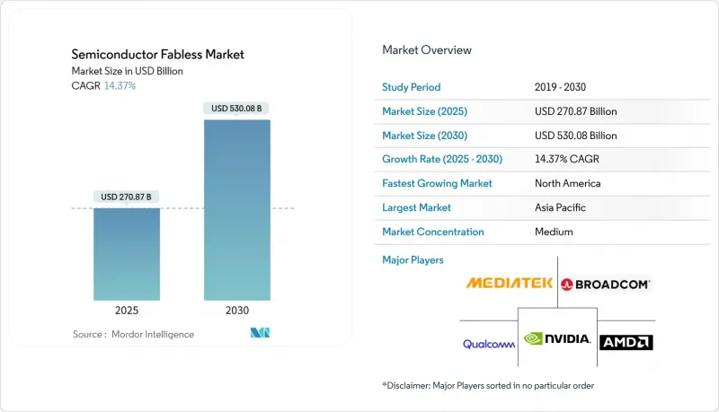
Mordor Intelligence에 의하면, 반도체 팹리스 시장 규모는 2025년에 2,708억 7,000만 달러로 평가되었고, 2030년까지 5,300억 8,000만 달러로 확대될 전망이며, CAGR은 14.37%를 나타낼 것으로 예측됩니다.
본 보고서는 제품 유형별(아날로그 IC, 로직 IC 등), 최종 이용 산업별(모바일 및 소비자용 전자기기, 데이터센터 및 클라우드 컴퓨팅 등), 기술 노드별(28 nm 이상, 16-22 nm 등), 고객 유형별(Tier 1 시스템 OEM, 신흥 디바이스 OEM 등), 지역별(북미, 남미 등)로 분류되어 있습니다. 시장 전망은 금액(달러) 기준으로 제시되어 있습니다.
세계의 반도체 팹리스 시장 동향 및 인사이트
생성형 AI의 컴퓨팅 슈퍼사이클이 하이엔드 로직 IC 수요를 끌어올리고 있다.
기업 내 대규모 언어 모델 서비스 도입은 데이터센터 아키텍처를 재구축하고 있으며, 예산은 도메인 특화형 프로세서, 텐서 가속기 및 고대역폭 메모리 칩렛으로 배분되고 있습니다. SEMI의 예측에 따르면, 2026년까지 AI용 반도체가 최첨단 웨이퍼 생산 능력 전체의 35%를 차지할 것으로 보이며, 이에 따라 주요 파블리스 기업들은 5nm 이하 공정공급을 확보하기 위해 수년에 걸친 파운드리 계약 체결을 추진하고 있습니다. 현재 경쟁 우위는 트랜스포머에 최적화된 코어, 저정밀 연산, 온다이 상호 연결 패브릭을 아우르는 IP 포트폴리오에 달려 있습니다. 이러한 요건은 하드웨어와 소프트웨어 스택을 공동 설계할 수 있는 기업에 유리하게 작용하며, 파브리스 반도체 시장이 AI 혁신의 선두주자로서의 입지를 더욱 공고히 하고 있습니다.
EV 및 ADAS 플랫폼에서의 자동차용 반도체 탑재량 확대
배터리식 전기차(BEV) 및 레벨 2 이상의 운전 지원 시스템으로 인해, 차량 1대당 반도체 탑재 가치는 지속적으로 증가하고 있습니다. 반도체산업협회(SIA)의 추정에 따르면, 와이드 밴드갭 파워 디바이스 및 기능 안전 규격을 준수하는 시스템 온 칩(SoC)의 보급에 힘입어, 자동차용 반도체는 2029년까지 연평균 두 자릿수 성장률을 나타낼 것으로 전망됩니다. 팹리스 기업들은 배터리 관리, 도메인 컨트롤러, 센서 퓨전 설계 분야에서 중요한 틈새 시장을 점유하고 있으며, IP 재사용에 유연성이 부족한 기존 Tier 1 공급업체로부터 수주를 확보하고 있습니다. 긴 인증 주기와 ISO 26262의 문서화 요건이 전환 비용을 발생시켜 설계 수주를 공고히 하는 동시에, 파브리스 반도체 시장의 상승 추세를 뒷받침하고 있습니다.
심각한 첨단 패키징 생산 능력 부족
ASE 그룹의 보고에 따르면, 2.5D 인터포저 및 팬아웃 웨이퍼 레벨 패키징의 가동률은 95%를 지속적으로 상회하고 있으며, 리드타임은 6개월 이상에 달하고 있습니다. AI 가속기나 치플릿 기반 네트워크 프로세서에는 이러한 패키징 형식이 필수적이기 때문에 공급 부족은 할당량을 둘러싼 경쟁과 프리미엄 가격 책정으로 이어지고 있습니다. 전용 라인을 확보하지 못한 팹리스 기업들은 성능이 더 낮은 패키지를 채택하여 설계를 재검토하거나 양산 시작을 늦출 수밖에 없으며, 그 결과 반도체 팹리스 시장의 당면한 수익 전망이 축소될 것입니다.
부문 분석
2024년, 로직 IC 매출액은 42.58%를 차지했으며, 반도체 팹리스 시장에서 가장 큰 점유율을 기록했습니다. 도메인 특화형 가속기, 임베디드 FPGA 및 이종 칩렛에 대한 수요가 급증함에 따라, 이 부문의 2030년까지 연평균 성장률(CAGR)은 15.28%로, 다른 모든 제품군을 상회하고 있습니다. 트랜스포머 추론, 보안 엔클레이브 코프로세서 및 고속 SerDes에 대한 집중이 장기적인 설계 프로젝트와 차별화된 IP 라이브러리 배포를 촉진하고 있습니다.
아날로그, MCU, MPU 각 카테고리는 전원 관리 및 엣지 제어 분야에서 여전히 필수적이지만, 성장률은 비교적 완만합니다. RF 및 혼합 신호 설계 기업들은 5G 및 Wi-Fi 7의 확산으로 이익을 얻고 있지만, AI 중심 로직이 보여주는 폭발적인 성장 궤적에는 미치지 못하는 상황입니다. 전반적으로 제품 구성의 변화로 인해 반도체 팹리스 시장 매출에서 로직 혁신이 차지하는 비중이 증가하고 있으며, 최첨단 노드에 대한 의존도가 높아지고 있습니다.
모바일 및 소비자 가전 분야는 여전히 최대의 용도 분야로, 2024년 매출의 38.63%를 차지했지만, 휴대전화 교체 주기가 길어짐에 따라 출하량 증가세는 둔화되고 있습니다. 대조적으로, 하이퍼스케일 사업자와 엔터프라이즈 IaaS 제공업체는 AI 훈련 클러스터에 두 자릿수 예산을 투자하고 있으며, 데이터센터 수요를 연평균 성장률(CAGR) 15.49%로 견인하고 있습니다.
서버급 가속기는 평균 판매 가격이 높기 때문에 매출 레버리지 효과가 확대되어, 반도체 팹리스 시장은 출하 대수당 가치를 상대적으로 높게 확보할 수 있게 되었습니다. 전기 구동용 인버터 및 ADAS 컨트롤러와 같은 자동차 분야의 설계 채택은 고객 기반을 확대하고 있으며, 한편 산업용 및 의료용 분야의 요구 사항은 긴 제품 수명 주기와 엄격한 인증 요건에 힘입어 규모는 작지만 안정적인 수익원이 되고 있습니다.
지역별 분석
2024년, 아시아태평양은 밀집된 제조 클러스터, 성숙한 EMS(전자기기 수탁 제조) 파트너십, 그리고 소비자용 기기 조립 라인과의 근접성을 활용하여 반도체 팹리스 시장 매출의 54.01%를 차지했습니다. 대만과 한국이 5nm 미만 웨이퍼의 대부분을 공급하는 한편, 일본은 전략적 리스크 분산을 도모하기 위해 특수 공정 및 3D 패키징 생산 능력을 확대되고 있습니다. 중국은 수출 규제라는 역풍 속에서도 14nm 및 28nm 라인에 대한 국내 투자를 가속화하고 있으며, 이로 인해 현지 팹리스 기업들은 중규모 AI 및 산업용 IoT 설계를 목표로 삼아야 하는 상황에 놓여 있습니다.
북미의 반도체 팹리스 시장은 ‘CHIPS 법’에 따른 인센티브, 견고한 소프트웨어 생태계, 하이퍼스케일 클라우드에 대한 투자에 힘입어 연평균 성장률(CAGR) 14.39%로 성장할 것으로 전망됩니다. 애리조나주, 텍사스주, 뉴욕주에서 진행 중인 파운드리 프로젝트로 인해 프로토타입에서 양산까지의 주기가 단축되고, 자동차, 항공우주, 방위 분야 계약공급망 안정성이 향상될 전망입니다. 또한, RISC-V 연산 블록 및 포토닉 IC 스타트업 기업을 대상으로 한 활발한 벤처 자금 조달로 인해 국내 설계 자원이 확대되고 있습니다.
유럽 시장 점유율은 다소 낮지만, 자동차용 전자기기, 공장 자동화, 보안 ID 솔루션과 같은 프리미엄 틈새 시장을 장악하고 있습니다. '유럽 칩 법'에 따른 430억 유로(500억 9,000만 달러) 규모의 자금 지원 방안은 새로운 2nm 파일럿 라인 및 용도 연구센터를 뒷받침하고 있으며, 예측 기간 동안 유럽의 반도체 생산 규모를 두 배로 늘리는 것을 목표로 하고 있습니다. 에너지 가격 변동과 인력 부족은 여전히 제약 요인으로 작용하고 있지만, 미국 및 아시아 파운드리와의 제휴를 통해 당장의 생산 능력 부족을 완화하고 있습니다.
기타 혜택 :
- Excel 형식 시장 예측(ME) 시트
- 3개월간의 애널리스트 지원
자주 묻는 질문
목차
제1장 서론
제2장 분석 방법
제3장 주요 요약
제4장 시장 구도
제5장 시장 규모 및 성장률 예측
제6장 경쟁 구도
제7장 시장 기회 및 향후 전망
AJY 26.08.07According to Mordor Intelligence, the semiconductor fabless market size reached USD 270.87 billion in 2025 and is projected to increase to USD 530.08 billion by 2030, growing at a 14.37% CAGR.
This report is Segmented by Product Type (Analog ICs, Logic ICs, and More), End-Use Industry (Mobile and Consumer Electronics, Data Center and Cloud Computing, and More), Technology Node (>=28 Nm, 16-22 Nm, and More), Customer Type (Tier-1 System OEMs, Emerging Device OEMs, and More), and Geography (North America, South America, and More). The Market Forecasts are Provided in Terms of Value (USD).
Global Semiconductor Fabless Market Trends and Insights
Generative AI Compute Super-Cycle Boosting High-End Logic IC Demand
Enterprise rollouts of large-language-model services are reshaping data-center architecture, channeling budget toward domain-specific processors, tensor accelerators, and high-bandwidth memory chiplets. SEMI projects that AI silicon will consume 35% of total leading-edge wafer capacity by 2026, prompting fabless leaders to secure multi-year foundry agreements to safeguard their sub-5 nm supply. Competitive pressure now hinges on IP portfolios covering transformer-optimized cores, low-precision arithmetic, and on-die interconnect fabrics. These requirements favor firms able to co-design hardware with software stacks, further entrenching the Semiconductor fabless market as the pace-setter for AI innovation.
Automotive Semiconductor Content Expansion in EV and ADAS Platforms
Battery-electric vehicles and Level 2+ driver-assistance systems continue to increase silicon value per car. The Semiconductor Industry Association estimates that automotive semiconductors will post double-digit annual growth through 2029, helped by wide-bandgap power devices and functional-safety-compliant system-on-chips. Fabless suppliers occupy key niches in battery management, domain controller, and sensor fusion designs, winning business from traditional tier-1s that lack agile IP reuse. Long qualification cycles and ISO 26262 documentation create switching costs, locking in design wins and reinforcing the upward trajectory of the Semiconductor fabless market.
Acute Advanced-Packaging Capacity Shortage
ASE Group reports that utilization for 2.5D interposers and fan-out wafer-level packaging remains above 95%, with lead times extending beyond six months. AI accelerators and chiplet-based network processors require these formats, so shortages translate into allocation battles and premium pricing. Fabless firms lacking captively reserved lines must redesign around less advanced packages or delay ramps, trimming immediate revenue potential for the Semiconductor fabless market.
Other drivers and restraints analyzed in the detailed report include:
- 5G and Wi-Fi 7 Transition Raising RF-Front-End IC Volumes
- Government CHIPS-Like Subsidies Accelerating Regional Design Hubs
- Geopolitical Export Controls Limiting Access to <7 nm Foundry Nodes
For complete list of drivers and restraints, kindly check the Table Of Contents.
Segment Analysis
Logic IC revenue represented the largest slice of the Semiconductor fabless market in 2024 at 42.58%. The segment's 15.28% CAGR through 2030 outpaces every other product class as demand for domain-specific accelerators, embedded FPGAs, and heterogeneous chiplets surges. The orientation toward transformer inference, secure enclave coprocessors, and high-speed SerDes encourages long design engagements and differentiated IP libraries.
The Analog, MCU, and MPU categories remain vital for power management and edge control, but they grow at more moderate rates. RF and mixed-signal design houses profit from the rollouts of 5G and Wi-Fi 7, yet they cannot match the explosive trajectory of AI-centric logic. Overall, the product mix shift ensures the Semiconductor fabless market receives an increasing proportion of its revenue from logic innovations, reinforcing dependency on leading-edge nodes.
Mobile and consumer electronics remained the largest application group, accounting for 38.63% of 2024 revenue; however, rising handset replacement intervals are tempering unit growth. In contrast, hyperscale operators and enterprise IaaS providers are investing double-digit budgets in AI training clusters, driving data-center demand at a 15.49% CAGR.
The higher average selling price profile of server-class accelerators magnifies revenue leverage, helping the Semiconductor fabless market capture disproportionate value per unit shipped. Automotive design wins for electric-drive inverters and ADAS controllers broaden the customer base, while industrial and medical requirements add smaller but stable streams anchored by long product lifecycles and stringent certification needs.
Complete Report Scope:
- By Product Type
- Analog ICs
- Logic ICs
- MCU and MPU
- RF AND Mixed-Signal ICs
- By End-Use Industry
- Mobile and Consumer Electronics
- Data Center and Cloud Computing
- Automotive and Transportation
- Industrial and Medical
- By Technology Node
- >=28 nm
- 16-22 nm
- 7-14 nm
- <7 nm
- By Customer Type
- Tier-1 System OEMs
- Emerging Device OEMs
- IP Licensing AND Design-Service Firms
- Government AND Defense Agencies
- By Technology
- Virtual Desktop Infrastructure (VDI)
- Application Virtualization
- Session Virtualization / Terminal Services
- Access Management and Monitoring
- By Geography
- North America
- United States
- Canada
- Mexico
- South America
- Brazil
- Argentina
- Rest of South America
- Europe
- Germany
- United Kingdom
- France
- Italy
- Spain
- Russia
- Rest of Europe
- Asia Pacific
- China
- Japan
- India
- South Korea
- Australia and New Zealand
- Rest of Asia Pacific
- Middle East
- Saudi Arabia
- United Arab Emirates
- Turkey
- Rest of Middle East
- Africa
- South Africa
- Nigeria
- Kenya
- Rest of Africa
- North America
Geography Analysis
The Asia Pacific generated 54.01% of the Semiconductor fabless market revenue in 2024, leveraging its dense manufacturing clusters, mature EMS relationships, and proximity to consumer device assembly lines. Taiwan and South Korea supply most sub-5 nm wafers, while Japan expands specialty processes and 3D packaging capacity to rebalance strategic exposure. China accelerates domestic investment in 14nm and 28nm lines amid export-control headwinds, pushing local fabless firms to target mid-range AI and industrial IoT designs.
North America's semiconductor fabless market is projected to grow at a 14.39% CAGR, driven by CHIPS Act incentives, a robust software ecosystem, and hyperscale cloud investment. Foundry projects in Arizona, Texas, and New York promise closer prototype-to-production loops, improving supply-chain certainty for automotive, aerospace, and defense contracts. Additionally, active venture funding around RISC-V compute blocks and photonic IC start-ups expands the domestic design pool.
Europe commands a modest share but captures premium niches in automotive electronics, factory automation, and secure ID solutions. The European Chips Act's EUR 43 billion (USD 50.09 billion) funding scheme backs new 2 nm pilot lines and applied-research centers, aiming to double the continent's semiconductor footprint across the forecast horizon. Energy-price volatility and talent shortages remain constraints; however, partnerships with U.S. and Asian foundries help mitigate immediate capacity gaps.
- NVIDIA Corporation
- Qualcomm Incorporated
- Broadcom Inc.
- Advanced Micro Devices Inc.
- MediaTek Inc.
- Marvell Technology Inc.
- Novatek Microelectronics Corp.
- Realtek Semiconductor Corp.
- Will Semiconductor Co. Ltd.
- Monolithic Power Systems Inc.
- Cirrus Logic Inc.
- Synaptics Inc.
- Himax Technologies Inc.
- Silicon Motion Technology Corp.
- GigaDevice Semiconductor Inc.
- Socionext Inc.
- LX Semicon Co. Ltd.
- Tsinghua Unigroup Co. Ltd. (UNISOC)
- Allegro MicroSystems Inc.
- OmniVision Technologies LLC
Additional Benefits:
- The market estimate (ME) sheet in Excel format
- 3 months of analyst support
TABLE OF CONTENTS
1 INTRODUCTION
- 1.1 Study Assumptions and Market Definition
- 1.2 Scope of the Study
2 RESEARCH METHODOLOGY
3 EXECUTIVE SUMMARY
4 MARKET LANDSCAPE
- 4.1 Market Overview
- 4.2 Market Drivers
- 4.2.1 Generative AI Compute Super-Cycle Boosting High-End Logic IC Demand
- 4.2.2 Automotive Semiconductor Content Expansion in EV and ADAS Platforms
- 4.2.3 5G AND Wi-Fi 7 Transition Raising RF-Front-End IC Volumes
- 4.2.4 Government CHIPS-Like Subsidies Accelerating Regional Design Hubs
- 4.2.5 Open-Source RISC-V Ecosystem Lowering Entry Barriers for New Design Houses
- 4.2.6 AI-Driven EDA Tool Adoption Slashing Tape-Out Time and Cost
- 4.3 Market Restraints
- 4.3.1 Acute Advanced-Packaging Capacity Shortage
- 4.3.2 Geopolitical Export Controls Limiting Access to <7 nm Foundry Nodes
- 4.3.3 Design-Talent Shortfall and Rising Labor Costs
- 4.3.4 Increasing Design-for-Reliability Burden in Automotive and Medical SoCs
- 4.4 Industry Value Chain Analysis
- 4.5 Regulatory Landscape
- 4.6 Technological Outlook
- 4.7 Porter's Five Forces Analysis
- 4.7.1 Threat of New Entrants
- 4.7.2 Bargaining Power of Suppliers
- 4.7.3 Bargaining Power of Buyers
- 4.7.4 Threat of Substitutes
- 4.7.5 Intensity Competitive Rivalry
- 4.8 Impact of Macroeconomic Factors on the Market
5 MARKET SIZE AND GROWTH FORECASTS (VALUE)
- 5.1 By Product Type
- 5.1.1 Analog ICs
- 5.1.2 Logic ICs
- 5.1.3 MCU and MPU
- 5.1.4 RF AND Mixed-Signal ICs
- 5.2 By End-Use Industry
- 5.2.1 Mobile and Consumer Electronics
- 5.2.2 Data Center and Cloud Computing
- 5.2.3 Automotive and Transportation
- 5.2.4 Industrial and Medical
- 5.3 By Technology Node
- 5.3.1 >=28 nm
- 5.3.2 16-22 nm
- 5.3.3 7-14 nm
- 5.3.4 <7 nm
- 5.4 By Customer Type
- 5.4.1 Tier-1 System OEMs
- 5.4.2 Emerging Device OEMs
- 5.4.3 IP Licensing AND Design-Service Firms
- 5.4.4 Government AND Defense Agencies
- 5.5 By Technology
- 5.5.1 Virtual Desktop Infrastructure (VDI)
- 5.5.2 Application Virtualization
- 5.5.3 Session Virtualization / Terminal Services
- 5.5.4 Access Management and Monitoring
- 5.6 By Geography
- 5.6.1 North America
- 5.6.1.1 United States
- 5.6.1.2 Canada
- 5.6.1.3 Mexico
- 5.6.2 South America
- 5.6.2.1 Brazil
- 5.6.2.2 Argentina
- 5.6.2.3 Rest of South America
- 5.6.3 Europe
- 5.6.3.1 Germany
- 5.6.3.2 United Kingdom
- 5.6.3.3 France
- 5.6.3.4 Italy
- 5.6.3.5 Spain
- 5.6.3.6 Russia
- 5.6.3.7 Rest of Europe
- 5.6.4 Asia Pacific
- 5.6.4.1 China
- 5.6.4.2 Japan
- 5.6.4.3 India
- 5.6.4.4 South Korea
- 5.6.4.5 Australia and New Zealand
- 5.6.4.6 Rest of Asia Pacific
- 5.6.5 Middle East
- 5.6.5.1 Saudi Arabia
- 5.6.5.2 United Arab Emirates
- 5.6.5.3 Turkey
- 5.6.5.4 Rest of Middle East
- 5.6.6 Africa
- 5.6.6.1 South Africa
- 5.6.6.2 Nigeria
- 5.6.6.3 Kenya
- 5.6.6.4 Rest of Africa
- 5.6.1 North America
6 COMPETITIVE LANDSCAPE
- 6.1 Market Concentration
- 6.2 Strategic Moves
- 6.3 Market Share Analysis
- 6.4 Company Profiles (includes Global Level Overview, Market Level Overview, Core Segments, Financials as available, Strategic Information, Market Rank/Share for key companies, Products and Services, and Recent Developments)
- 6.4.1 NVIDIA Corporation
- 6.4.2 Qualcomm Incorporated
- 6.4.3 Broadcom Inc.
- 6.4.4 Advanced Micro Devices Inc.
- 6.4.5 MediaTek Inc.
- 6.4.6 Marvell Technology Inc.
- 6.4.7 Novatek Microelectronics Corp.
- 6.4.8 Realtek Semiconductor Corp.
- 6.4.9 Will Semiconductor Co. Ltd.
- 6.4.10 Monolithic Power Systems Inc.
- 6.4.11 Cirrus Logic Inc.
- 6.4.12 Synaptics Inc.
- 6.4.13 Himax Technologies Inc.
- 6.4.14 Silicon Motion Technology Corp.
- 6.4.15 GigaDevice Semiconductor Inc.
- 6.4.16 Socionext Inc.
- 6.4.17 LX Semicon Co. Ltd.
- 6.4.18 Tsinghua Unigroup Co. Ltd. (UNISOC)
- 6.4.19 Allegro MicroSystems Inc.
- 6.4.20 OmniVision Technologies LLC
7 MARKET OPPORTUNITIES AND FUTURE OUTLOOK
- 7.1 White-Space and Unmet-Need Assessment


