

|
시장보고서
상품코드
2099424
GPU 파운드리 : 시장 점유율 분석, 업계 동향 및 통계, 성장 예측(2026-2031년)GPU Foundry - Market Share Analysis, Industry Trends & Statistics, Growth Forecasts (2026 - 2031) |
||||||
 Mordor Intelligence
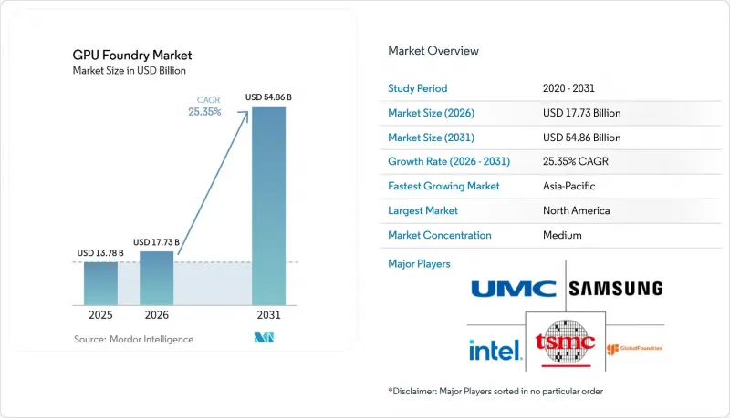
Mordor Intelligence에 의하면, GPU 파운드리 시장 규모는 2025년 137억 8,000만 달러로 평가되었습니다. 2026년에는 177억 3,000만 달러로 확대되어 2031년까지 548억 6,000만 달러에 이를 것으로 예상되고 2026년부터 2031년에 걸쳐 CAGR 25.35%로 성장할 전망입니다.
본 보고서는 기술 노드(3nm 이하, 4/5nm, 6/7nm, 8/10/12nm, 14/16nm, 20/22/28nm, 기타), 웨이퍼 크기(300mm, 200mm, 기타), 파운드리 비즈니스 모델(퓨어플레이 파운드리, IDM 머천트 파운드리 서비스), 용도(데이터센터용 AI 및 HPC, 클라이언트 컴퓨팅 및 게임, 자동차, 산업용, 기타), 그리고 지역별로 분류되어 있습니다. 시장 전망은 금액(달러) 기준으로 제시되어 있습니다.
세계의 GPU 파운드리 시장 동향 및 인사이트
하이퍼스케일 AI 훈련 및 추론 클러스터의 확대
클라우드 플랫폼이 AI 처리 능력을 확충하는 한편, 기업 고객들도 추론 이용 사례를 확대함에 따라, 하이퍼스케일 분야에 대한 투자는 계속해서 GPU 파운드리 시장의 주요 수요원으로 자리 잡고 있습니다. 현재 GPU 파운드리 시장은 대규모 훈련 클러스터와 지속적인 추론 도입을 모두 지원하고 있으며, 이로 인해 하이엔드 웨이퍼 수요에서 일회성 조달 붐보다는 안정적인 보충 주기가 형성되고 있습니다. 이는 성능 요구 사항이 높아지고 서비스 지연 시간이 더욱 중요해짐에 따라, AI 시스템의 도입 기반을 업데이트, 확장 및 지역별로 복제해야 하기 때문에 중요한 의미를 지닙니다. 주요 클라우드 기업들의 자체 제작 가속기 확대는 더 많은 맞춤형 실리콘 프로그램이 첨단 노드의 생산 능력을 놓고 경쟁하게 되었음을 의미하며, 이는 GPU 파운드리 시장이 더 이상 단일 칩 설계 회사에 얽매이지 않게 되었음을 시사합니다. NVIDIA는 피닉스에서 Blackwell 웨이퍼 생산이 진행 중이며, 파트너 기업들과 함께 미국에서 최대 5,000억 달러 상당의 AI 인프라를 생산할 계획이라고 발표했습니다. 이는 현재 AI 수요가 최첨단 웨이퍼 생산 개시와 하류 시스템 제조 능력 모두를 견인하고 있음을 보여줍니다.
엔터프라이즈 AI 팩토리 및 소버린 컴퓨트 조달
엔터프라이즈 AI 팩토리 프로그램과 소버린 컴퓨트 계획을 통해 GPU 파운드리 시장에는 순수한 상업적 최적화에 대한 의존도가 낮은 보다 광범위한 수요 기반이 형성되고 있습니다. 조달은 회복탄력성, 국내 생산 지향, 그리고 신뢰할 수 있는 공급원에 대한 필요성에 의해 점점 더 형성되고 있으며, 이로 인해 여러 지역에 걸쳐 인증된 생산 능력을 제시할 수 있는 파운드리 업체의 가치가 높아지고 있습니다. TSMC는 2025년 3월, 미국에 대한 투자 계획을 1,650억 달러로 확대했습니다. 이 계획에는 3개의 신규 팹, 2개의 첨단 패키징 시설, 그리고 애리조나주에 건설될 대규모 연구개발 센터가 포함되어 있습니다. 또한 NVIDIA는 AI 인프라를 위한 미국 내 제조 네트워크가 현재 반도체, 기판, 시스템, 랙 등 각 분야에 걸친 파트너로 확대되고 있다고 밝혔으며, 이는 주권 및 기업 구매자들이 AI 하드웨어 스택에 대해 더 많은 현지 관리 권한을 요구하고 있다는 관점을 뒷받침합니다. 전 세계 파운드리 업체들은 시설 확장, 패키징 기술 혁신, 실리콘 포토닉스, 차세대 GaN에 초점을 맞춘 160억 달러 규모의 미국 투자를 발표하며 국내 시장에 대한 추가적인 참여를 시사했습니다. 이는 최첨단 기술 점유율이 여전히 집중되어 있는 분야라 하더라도, GPU 파운드리 시장 내 조달처가 다양화되고 있음을 뒷받침합니다.
수출 규제와 관세 변동
수출 규제는 최종 목적지 승인, 고객 구성 및 할당 계획에 동시에 영향을 미치기 때문에 GPU 파운드리 시장에 있어 여전히 가장 큰 외부 제약 요인으로 남아 있습니다. 미국 산업안보국(BIS)은 2026년 1월, 중국 및 마카오로의 특정 첨단 컴퓨팅 칩 수출에 관한 정책을 변경하여, 지정 제품에 대해 ‘원칙적으로 거부’에서 ‘사례별 심사’로 전환했습니다. 이 방침에 따라 수출업체는 미국 최종 사용자를 위한 유사하거나 더 고도화된 칩의 전 세계 파운드리 생산 능력이 전용되지 않음을 입증해야 하며, 이로 인해 파운드리 할당이 수출 규정 준수와 직접적으로 연계되고 있습니다. 그 결과, GPU 파운드리 시장에서는 서류 작성 및 심사가 증가했으며, 어떤 첨단 제품이 지연 없이 생산 라인을 통과할 수 있을지에 대한 불확실성이 높아지고 있습니다. 이러한 불확실성이 수요를 멈추게 하지는 않지만, GPU 파운드리 시장 전체에서 고객의 우선순위 설정, 생산 계획 및 수익 발생 시점 관리를 어렵게 만들고 있습니다.
부문 분석
2025년, 4/5nm 부문은 GPU 파운드리 시장 점유율의 42.11%를 차지했으며, 이러한 위상은 현재의 AI 가속기, 고성능 추론 칩 및 주요 클라우드 고객을 위한 맞춤형 실리콘의 주요 생산 세대를 반영한 것입니다. GPU 파운드리 시장에서 이 노드 대역은 이전 세대 노드나 차세대 노드의 초기 단계보다 트랜지스터 밀도, 수율 성숙도, 생태계 구축 현황의 균형이 뛰어나기 때문에 여전히 상업적 중심을 이루고 있습니다. 또한, 패키징, 소프트웨어, 시스템 설계가 준비되기 전에 모든 고객에게 가장 비용이 많이 드는 노드를 강요하지 않으면서도 플래그십 AI 제품을 대규모로 생산할 수 있는 지점에 위치해 있습니다. 6/7nm 및 8/10/12nm와 같은 성숙한 노드군은 게임 제품, 클라이언트용 그래픽스, 자동차용 컨트롤러, 산업용 추론 디바이스가 여전히 긴 리프레시 주기로 출하되고 있기 때문에 GPU 파운드리 시장에서 여전히 중요한 역할을 수행하고 있습니다.
3nm 이하 부문은 2031년까지 연평균 성장률(CAGR) 26.21%로 확대될 것으로 예측되며, GPU 파운드리 시장이 전력 효율이 더 높은 AI 컴퓨팅으로 전환됨에 따라 이 부문이 가장 빠르게 성장하는 노드 카테고리가 될 것입니다. NVIDIA와 TSMC는 첫 번째 Blackwell 웨이퍼가 피닉스에서 생산되었으며, TSMC 애리조나 공장에서 2nm, 3nm, 4nm 및 A16 기술을 생산할 것이라고 발표했습니다. 이는 최첨단 AI 제품과 확대되는 5nm 미만 제조 거점 간의 실질적인 연계성을 뒷받침하는 것입니다. 인텔은 Intel 18A가 2025년에 양산에 들어가고, Intel 18A-P가 2026년에 리스크 생산에 들어갈 것이라고 밝히며 추가적인 신호를 보냈습니다. 이는 현재 GPU 파운드리 시장이 여전히 집중되어 있더라도, 미래의 최첨단 기술을 둘러싼 경쟁이 더욱 현실화되고 있음을 보여줍니다. 실제로 GPU 파운드리 업계는 4/5nm가 여전히 큰 상업적 기반을 형성하고, 3nm 이하가 프리미엄 AI로의 전환을 주도하며, 성숙한 노드가 비용 효율성을 중시하고 인증 요건이 엄격한 제품을 계속해서 담당하는 계층화된 노드 구조로 운영될 가능성이 높습니다. 이는 GPU 파운드리 시장이 구형 노드에서 완전히 벗어난 것은 아니지만, 설계 복잡도와 가격 결정력이 가장 강한 첨단 노드 계층에 가치 성장의 더 큰 부분을 두고 있음을 의미합니다.
2025년 시점에서 300mm 부문은 GPU 파운드리 시장 규모의 96.33%를 차지했으며, 2031년까지 연평균 성장률(CAGR)이 26.62%로 가장 빠르게 성장하고 있는 웨이퍼 크기 부문이기도 합니다. 이러한 우위는 GPU 파운드리 시장이 대형 다이 설계, 1회 제조당 생산량 증대, 그리고 고가의 첨단 노드 생산 능력의 효율적인 활용 측면에서 300mm의 경제성에 의존하고 있기 때문에 예상되는 것입니다. GPU 파운드리 업계에서 200mm 웨이퍼를 이용한 생산은 특수 컨트롤러, 전원 부품, 그리고 대형 웨이퍼로의 전환을 통해 충분한 수익 향상을 기대하기 어려운 구형 그래픽스 관련 디바이스 분야에서 여전히 일정한 역할을 수행하고 있습니다. 150mm 이하 부문은 GPU 파운드리 시장에서 여전히 미미한 비중을 차지하며, 주류인 GPU 웨이퍼 제조라기보다는 주로 기판 및 관련 부품 제조에 국한되어 있습니다.
GPU 파운드리 시장에서 300mm 웨이퍼의 중요성은 프런트엔드 로직 제조에 그치지 않고, 최신 AI 디바이스를 뒷받침하는 광범위한 패키징 생태계까지 미치고 있습니다. TSMC는 애리조나주 확장 계획에 2개의 첨단 패키징 시설이 포함되어 있다고 발표했으며, 이는 웨이퍼 제조와 백엔드 통합 양면에서 300mm 기반이 강화되고 있음을 의미합니다. 전 세계 파운드리 업체들도 미국 내 패키징 혁신과 실리콘 포토닉스에 대한 자금 지원을 약속하고 있으며, 이는 국내 반도체 전략이 단순한 독립형 팹 시설뿐만 아니라 더 광범위한 제조 체인을 중심으로 구축되고 있음을 보여줍니다. 그 결과, GPU 파운드리 시장은 공정 성숙도, 패키징 호환성, 생산 능력에 대한 투자가 모두 유기적으로 진행되고 있는 300mm 인프라에 앞으로도 압도적으로 의존할 가능성이 높다고 볼 수 있습니다.
지역별 분석
2025년, 북미는 GPU 파운드리 시장 점유율의 68.44%를 차지했으며, 이러한 우위는 최첨단 수요의 대부분을 주도하는 팹리스 AI 칩 설계 기업, 하이퍼스케일러, 시스템 개발 기업이 해당 지역에 집중되어 있기 때문입니다. 따라서 북미의 GPU 파운드리 시장은 웨이퍼 제조의 대부분이 역사적으로 동아시아에 집중되어 있음에도 불구하고, 수요와 설계가 중심이 되고 있습니다. TSMC는 2025년 3월, 미국 내 투자 계획을 1,650억 달러로 확대했으며, 이 계획에는 3개의 신규 팹, 2개의 첨단 패키징 시설, 그리고 애리조나주에 위치한 대규모 연구개발 센터가 포함되어 있습니다. 또한 NVIDIA는 피닉스에서 Blackwell 웨이퍼 생산이 진행 중이며, 파트너 기업과 협력하여 미국에서 최대 5,000억 달러 상당의 AI 인프라를 생산할 계획이라고 밝혔습니다. 이는 해당 지역의 사업 전개가 실리콘 설계에서 물리적 제조 및 시스템 구축으로 확대되고 있음을 보여줍니다. 이로 인해 국경을 초월한 제조에 대한 의존도가 여전히 중요한 전략적 위험 요인으로 남아 있음에도 불구하고, 북미는 GPU 파운드리 시장의 상업적 중심지가 되었습니다.
아시아태평양은 연평균 성장률(CAGR) 26.42%로 확대될 것으로 예측되며, 2031년까지 GPU 파운드리 시장 규모 측면에서 가장 빠르게 성장하는 지역이 될 전망입니다. 이 지역의 GPU 파운드리 시장은 최첨단 제조 분야에서 대만이 중심적인 역할을 하고 있는 데 힘입고 있지만, 일본, 한국, 인도와 관련된 투자 흐름에 힘입어 그 범위도 확대되고 있습니다. 캐드런스와 삼성 파운드리(Samsung Foundry)는 2026년, 2nm 및 3D-IC 분야에서의 협력을 심화했습니다. 이는 차세대 AI의 설계 및 제조 공정에서 한국이 계속해서 중요한 위치를 유지하려는 노력을 뒷받침하는 것입니다. 이 지역의 GPU 파운드리 시장 성장 요인은 시장 규모, 탄탄한 공급망, 그리고 실용적인 첨단 노드 제조 역량의 상당 부분이 여전히 이 지역에 집중되어 있다는 사실에 있습니다.
유럽은 여전히 GPU 파운드리 시장에서 비교적 작은 점유율을 차지하고 있지만, 정책 지원, 신뢰성 높은 제조 체계, 그리고 특수 반도체 기술 역량을 통해 그 중요성을 높여가고 있습니다. 전 세계 파운드리 업체들은 2025년, 패키징 및 포토닉스 사업 확장을 포함해 160억 달러 규모의 투자를 발표했는데, 이러한 산업 정책에 대한 대응은 동맹국 지역 전체에 걸쳐 탄탄한 반도체 생산 능력을 확보하기 위한 광범위한 노력을 반영하고 있습니다. 남미, 중동 및 아프리카는 여전히 GPU 파운드리 시장에서 점유율이 제한적이지만, 중동은 국가 주도의 AI 인프라 수요 거점으로서 중요성이 커지고 있습니다. 이 지역들이 GPU 파운드리 시장에서 수행할 장기적인 역할은 단기적인 국내 대규모 최첨단 팹 생산 능력 구축보다는 오히려 컴퓨팅 도입, 연결성 향상, 그리고 신뢰할 수 있는 조달 파트너십에 크게 좌우될 가능성이 높다고 볼 수 있습니다.
기타 혜택 :
- 엑셀 형식 시장 예측(ME) 시트
- 3개월간의 애널리스트 지원
자주 묻는 질문
목차
제1장 서론
제2장 조사 방법
제3장 주요 요약
제4장 시장 구도
제5장 시장 규모 및 성장 예측
제6장 경쟁 구도
제7장 시장 기회 및 향후 전망
KTH 26.08.10According to Mordor Intelligence, the GPU foundry market size is expected to increase from USD 13.78 billion in 2025 to USD 17.73 billion in 2026 and reach USD 54.86 billion by 2031, growing at a CAGR of 25.35% over 2026-2031.
This report is Segmented by Technology Node (3 Nm and Below, 4/5 Nm, 6/7 Nm, 8/10/12 Nm, 14/16 Nm, 20/22/28 Nm, and More), Wafer Size (300 Mm, 200 Mm, and More), Foundry Business Model (Pure-Play Foundry, and IDM Merchant Foundry Services), Application (Data Center AI and HPC, Client Computing and Gaming, Automotive, Industrial, and More), and Geography. The Market Forecasts are Provided in Terms in Value (USD).
Global GPU Foundry Market Trends and Insights
Hyperscale AI Training and Inference Cluster Expansion
Hyperscale spending remains the main demand engine for the GPU foundry market because cloud platforms are building AI capacity at the same time that enterprise customers are broadening inference use cases. The GPU foundry market now supports both large training clusters and recurring inference deployments, and that creates a steadier replenishment cycle for high-end wafer demand than one-off procurement waves. This matters because the installed base of AI systems has to be refreshed, expanded, and regionally duplicated as performance requirements rise and service latency becomes more important. The growth of in-house accelerators at major cloud firms also means the GPU foundry market is no longer tied to a single chip designer, since more custom silicon programs now compete for advanced-node capacity. NVIDIA stated that Blackwell wafer production is underway in Phoenix and that it plans to produce up to USD 500 billion of AI infrastructure in the US with partners, which shows how AI demand is now pulling on both leading-edge wafer starts and downstream system manufacturing capacity.
Enterprise AI Factory and Sovereign Compute Procurement
Enterprise AI factory programs and sovereign compute plans are giving the GPU foundry market a broader demand base that is less dependent on pure commercial optimization. Procurement is increasingly shaped by resilience, domestic production preferences, and the need for trusted supply, which raises the value of foundries that can point to certified capacity across more than one geography. TSMC expanded its planned US investment to USD 165 billion in March 2025, and that package includes three new fabs, two advanced packaging facilities, and a major R&D center in Arizona.NVIDIA also said its US manufacturing network for AI infrastructure now spans partners across semiconductors, boards, systems, and racks, which supports the view that sovereign and enterprise buyers want more local control over the AI hardware stack. GlobalFoundries added another domestic signal with a USD 16 billion US investment focused on facility expansion, packaging innovation, silicon photonics, and next-generation GaN, and that supports a wider sourcing field inside the GPU foundry market even where leading-edge share remains concentrated.
Export Controls and Tariff Volatility
Export controls remain the most disruptive external restraint for the GPU foundry market because they affect end-destination approval, customer mix, and allocation planning at the same time. The US Bureau of Industry and Security changed its policy on certain advanced computing chip exports to China and Macau in January 2026, shifting from a presumption of denial to a case-by-case review for specified products. That policy also requires exporters to certify that global foundry capacity for similar or more advanced chips for US end users will not be diverted, which ties foundry allocation directly to export compliance. The result is that the GPU foundry market faces more documentation, more screening, and less certainty around which advanced products can move through the pipeline without delay. This uncertainty does not stop demand, but it does make customer prioritization, production planning, and revenue timing harder to manage across the GPU foundry market.
Other drivers and restraints analyzed in the detailed report include:
- AI Accelerator Race for Sub-5 Nm Advanced Nodes
- Chiplet-Based GPU Roadmaps Improving Yield and Product Scaling
- HBM and Advanced Packaging Allocation Bias Toward AI Racks
For complete list of drivers and restraints, kindly check the Table Of Contents.
Segment Analysis
The 4/5 nm segment held 42.11% of the GPU foundry market share in 2025, and that position reflected the main production generation for current AI accelerators, high-performance inference chips, and custom silicon from large cloud customers. In the GPU foundry market, this node band remains the commercial center because it balances transistor density, yield maturity, and ecosystem readiness better than older nodes and better than very early next-generation ramps. It also sits at the point where flagship AI products can be produced at scale without forcing every customer onto the highest-cost node before packaging, software, and system design are ready. Mature clusters such as 6/7 nm and 8/10/12 nm still matter in the GPU foundry market because gaming products, client graphics, automotive controllers, and industrial inference devices continue to ship on longer refresh cycles.
The 3 nm and below segment is projected to expand at a 26.21% CAGR through 2031, and that makes it the fastest node category as the GPU foundry market moves toward more power-efficient AI compute. NVIDIA and TSMC said the first Blackwell wafer was produced in Phoenix and that TSMC Arizona will produce 2 nm, 3 nm, 4 nm, and A16 technologies, which reinforces the practical link between advanced AI products and a widening sub-5 nm manufacturing footprint. Intel added another signal when it said Intel 18A entered production in 2025 and Intel 18A-P entered risk production in 2026, which shows that future leading-edge competition is becoming more credible even if the current GPU foundry market remains concentrated. In practice, the GPU foundry industry is likely to run with a layered node structure where 4/5 nm remains a large commercial base, 3 nm and below captures the premium AI migration, and mature nodes keep serving cost-sensitive and qualification-heavy products. This means the GPU foundry market is not moving away from older nodes entirely, but it is placing more of its value growth in the advanced-node tier where design complexity and pricing power are strongest.
The 300 mm segment commanded 96.33% of GPU foundry market size in 2025, and it also stands as the fastest-growing wafer size segment with a 26.62% CAGR through 2031. That dominance is expected because the GPU foundry market relies on 300 mm economics for large die designs, better output per run, and more efficient use of expensive advanced-node capacity. In the GPU foundry industry, 200 mm production still has a role in specialty controllers, power components, and older graphics-related devices where migration to larger wafers would not improve returns enough to justify the shift. The 150 mm and below tier remains marginal in the GPU foundry market and is mainly tied to supporting substrates or adjacent components rather than mainstream GPU wafer fabrication.
The importance of 300 mm wafers in the GPU foundry market extends beyond front-end logic production and into the broader packaging ecosystem that supports modern AI devices. TSMC said its Arizona expansion includes two advanced packaging facilities, which means the 300 mm footprint is being reinforced across both wafer fabrication and back-end integration. GlobalFoundries also committed funding to packaging innovation and silicon photonics in the US, which shows that domestic semiconductor strategy is being built around broader manufacturing chains and not just standalone fab shells. As a result, the GPU foundry market is likely to remain overwhelmingly tied to 300 mm infrastructure because that is where process maturity, packaging compatibility, and capacity investment are all moving together.
Complete Report Scope:
- By Technology Node
- 3 Nm and Below
- 4/5 Nm
- 6/7 Nm
- 8/10/12 Nm
- 14/16 Nm
- 20/22/28 Nm
- 40/45/55 Nm
- 65 Nm and Above
- By Wafer Size
- 300 Mm
- 200 Mm
- 150 Mm and Below
- By Foundry Business Model
- Pure-Play Foundry
- IDM Merchant Foundry Services
- By Application
- Data Center AI and HPC
- Client Computing and Gaming
- Professional Visualization and Workstations
- Automotive
- Industrial, Edge AI, IoT, and Robotics
- Consumer Electronics and Mobile Graphics
- Other Applications
- By Geography
- North America
- United States
- Canada
- Mexico
- Europe
- Germany
- United Kingdom
- France
- Italy
- Rest of Europe
- Russia
- Asia-Pacific
- China
- Japan
- South Korea
- India
- Southeast Asia
- Rest of Asia-Pacific
- South America
- Brazil
- Argentina
- Rest of South America
- Middle East
- Saudi Arabia
- United Arab Emirates
- Turkey
- Rest of Middle East
- Africa
- South Africa
- Rest of Africa
- North America
Geography Analysis
North America held 68.44% of the GPU foundry market share in 2025, and that lead came from the region's concentration of fabless AI chip designers, hyperscalers, and system developers that drive most leading-edge demand. The GPU foundry market in North America is therefore demand-heavy and design-heavy, even though a large share of wafer fabrication has historically remained concentrated in East Asia. TSMC expanded its planned US investment to USD 165 billion in March 2025, and the package covers three new fabs, two advanced packaging facilities, and a major RandD center in Arizona. NVIDIA also said Blackwell wafer production is underway in Phoenix and that it plans to produce up to USD 500 billion of AI infrastructure in the US with partners, which shows that the regional footprint is extending from silicon design into physical manufacturing and system buildout. This makes North America the commercial center of the GPU foundry market even as cross-border manufacturing dependence remains an important strategic risk.
Asia-Pacific is projected to expand at a 26.42% CAGR, making it the fastest-growing contributor to GPU foundry market size through 2031. The GPU foundry market in this region remains anchored by Taiwan's central role in leading-edge fabrication, but it is also being widened by investment paths linked to Japan, South Korea, and India. Cadence and Samsung Foundry deepened their 2 nm and 3D-IC collaboration in 2026, which supports South Korea's effort to stay relevant in next-generation AI design and manufacturing flows. The region's growth profile in the GPU foundry market comes from scale, supply chain depth, and the fact that most practical advanced-node manufacturing capacity is still clustered there.
Europe remains a smaller part of the GPU foundry market, but it is gaining relevance through policy support, trusted manufacturing, and specialty semiconductor capabilities. GlobalFoundries announced a USD 16 billion US investment in 2025 that included packaging and photonics expansion, and that kind of industrial policy response mirrors the broader push for resilient semiconductor capacity across allied regions. South America, the Middle East, and Africa still represent a limited share of the GPU foundry market, although the Middle East is becoming more important as a demand center for sovereign AI infrastructure. The long-term role of these regions in the GPU foundry market is likely to depend more on compute deployment, connectivity upgrades, and trusted sourcing partnerships than on near-term creation of large domestic leading-edge fab capacity.
- Taiwan Semiconductor Manufacturing Company Limited
- Samsung Electronics Co., Ltd.
- Intel Corporation
- GlobalFoundries Inc.
- United Microelectronics Corporation
- Semiconductor Manufacturing International Corporation
- Tower Semiconductor Ltd.
- Hua Hong Semiconductor Limited
- Powerchip Semiconductor Manufacturing Corporation
- Vanguard International Semiconductor Corporation
- X-FAB Silicon Foundries SE
- SkyWater Technology, Inc.
- STMicroelectronics N.V.
- Renesas Electronics Corporation
- Dongbu HiTek Co., Ltd.
- PSMC Group
- ASE Technology Holding Co., Ltd.
- Amkor Technology, Inc.
- JCET Group Co., Ltd.
- SMIC Shanghai Manufacturing Co.
Additional Benefits:
- The market estimate (ME) sheet in Excel format
- 3 months of analyst support
TABLE OF CONTENTS
1 INTRODUCTION
- 1.1 Study Assumptions and Market Definition
- 1.2 Scope of the Study
2 RESEARCH METHODOLOGY
3 EXECUTIVE SUMMARY
4 MARKET LANDSCAPE
- 4.1 Market Overview
- 4.2 Market Drivers
- 4.2.1 Hyperscale AI Training and Inference Cluster Expansion
- 4.2.2 Enterprise AI Factory and Sovereign Compute Procurement
- 4.2.3 Chiplet-Based GPU Roadmaps Improving Yield and Product Scaling
- 4.2.4 AI Accelerator Race for Sub-5 Nm Advanced Nodes
- 4.2.5 Industry Demand for Trusted Domestic Fabs
- 4.2.6 Foundry Capacity Lock-In Through Long-Term AI Supply Agreements
- 4.3 Market Restraints
- 4.3.1 Export Controls and Tariff Volatility
- 4.3.2 Elevated GPU and Memory ASPs Slowing Mainstream Adoption
- 4.3.3 HBM and Advanced Packaging Allocation Bias Toward AI Racks
- 4.3.4 Grid Interconnection Delays for High-Density GPU Campuses
- 4.4 Industry Value Chain Analysis
- 4.5 Industry Supply Chain Analysis
- 4.6 Impact of Macroeconomic Factors on the Market
- 4.7 Regulatory Landscape
- 4.8 Technological Outlook
- 4.9 Porter's Five Forces Analysis
- 4.9.1 Bargaining Power of Suppliers
- 4.9.2 Bargaining Power of Buyers
- 4.9.3 Threat of New Entrants
- 4.9.4 Threat of Substitutes
- 4.9.5 Intensity of Competitive Rivalry
5 MARKET SIZE AND GROWTH FORECASTS (VALUE)
- 5.1 By Technology Node
- 5.1.1 3 Nm and Below
- 5.1.2 4/5 Nm
- 5.1.3 6/7 Nm
- 5.1.4 8/10/12 Nm
- 5.1.5 14/16 Nm
- 5.1.6 20/22/28 Nm
- 5.1.7 40/45/55 Nm
- 5.1.8 65 Nm and Above
- 5.2 By Wafer Size
- 5.2.1 300 Mm
- 5.2.2 200 Mm
- 5.2.3 150 Mm and Below
- 5.3 By Foundry Business Model
- 5.3.1 Pure-Play Foundry
- 5.3.2 IDM Merchant Foundry Services
- 5.4 By Application
- 5.4.1 Data Center AI and HPC
- 5.4.2 Client Computing and Gaming
- 5.4.3 Professional Visualization and Workstations
- 5.4.4 Automotive
- 5.4.5 Industrial, Edge AI, IoT, and Robotics
- 5.4.6 Consumer Electronics and Mobile Graphics
- 5.4.7 Other Applications
- 5.5 By Geography
- 5.5.1 North America
- 5.5.1.1 United States
- 5.5.1.2 Canada
- 5.5.1.3 Mexico
- 5.5.2 Europe
- 5.5.2.1 Germany
- 5.5.2.2 United Kingdom
- 5.5.2.3 France
- 5.5.2.4 Italy
- 5.5.2.5 Rest of Europe
- 5.5.2.6 Russia
- 5.5.3 Asia-Pacific
- 5.5.3.1 China
- 5.5.3.2 Japan
- 5.5.3.3 South Korea
- 5.5.3.4 India
- 5.5.3.5 Southeast Asia
- 5.5.3.6 Rest of Asia-Pacific
- 5.5.4 South America
- 5.5.4.1 Brazil
- 5.5.4.2 Argentina
- 5.5.4.3 Rest of South America
- 5.5.5 Middle East
- 5.5.5.1 Saudi Arabia
- 5.5.5.2 United Arab Emirates
- 5.5.5.3 Turkey
- 5.5.5.4 Rest of Middle East
- 5.5.6 Africa
- 5.5.6.1 South Africa
- 5.5.6.2 Rest of Africa
- 5.5.1 North America
6 COMPETITIVE LANDSCAPE
- 6.1 Market Concentration
- 6.2 Strategic Moves
- 6.3 Market Positioning Analysis
- 6.4 Company Profiles (includes Global Level Overview, Market Level Overview, Core Segments, Financials as available, Strategic Information, Market Rank/Share, Products and Services, Recent Developments)
- 6.4.1 Taiwan Semiconductor Manufacturing Company Limited
- 6.4.2 Samsung Electronics Co., Ltd.
- 6.4.3 Intel Corporation
- 6.4.4 GlobalFoundries Inc.
- 6.4.5 United Microelectronics Corporation
- 6.4.6 Semiconductor Manufacturing International Corporation
- 6.4.7 Tower Semiconductor Ltd.
- 6.4.8 Hua Hong Semiconductor Limited
- 6.4.9 Powerchip Semiconductor Manufacturing Corporation
- 6.4.10 Vanguard International Semiconductor Corporation
- 6.4.11 X-FAB Silicon Foundries SE
- 6.4.12 SkyWater Technology, Inc.
- 6.4.13 STMicroelectronics N.V.
- 6.4.14 Renesas Electronics Corporation
- 6.4.15 Dongbu HiTek Co., Ltd.
- 6.4.16 PSMC Group
- 6.4.17 ASE Technology Holding Co., Ltd.
- 6.4.18 Amkor Technology, Inc.
- 6.4.19 JCET Group Co., Ltd.
- 6.4.20 SMIC Shanghai Manufacturing Co.
7 MARKET OPPORTUNITIES AND FUTURE OUTLOOK
- 7.1 White-Space and Unmet-Need Assessment


