

|
시장보고서
상품코드
2099495
연산-메모리 통합 : 시장 점유율 분석, 업계 동향 및 통계, 성장 예측(2026-2031년)Compute-Memory Integration - Market Share Analysis, Industry Trends & Statistics, Growth Forecasts (2026 - 2031) |
||||||
 Mordor Intelligence
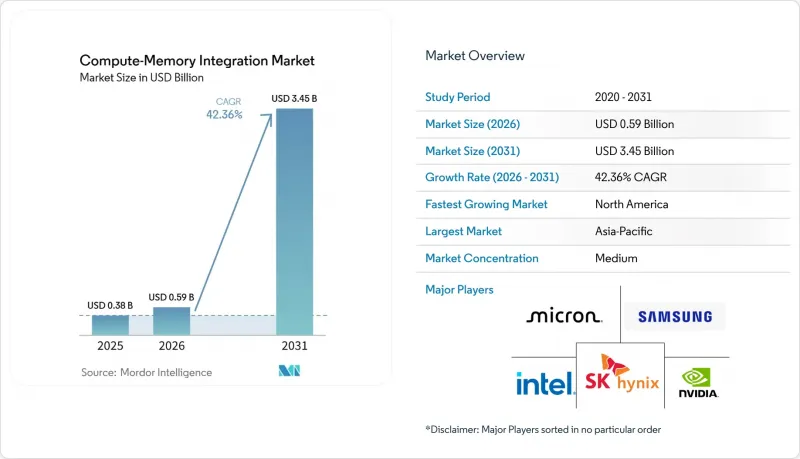
Mordor Intelligence에 의하면, 연산-메모리 통합 시장 규모는 2025년에 3억 8,000만 달러로 평가되었습니다. 2026년 5억 9,000만 달러, 2031년 34억 5,000만 달러에 이를 것으로 예측되며, 2026년부터 2031년에 걸쳐 CAGR 42.36%로 성장할 전망입니다.
본 보고서는 컴퓨팅 유형(아날로그, 연산-메모리 칩 등), 메모리 기술(SRAM 기반, DRAM/HBM 기반 PIM 등), 적용 환경(엣지 디바이스, 데이터센터 및 하이퍼스케일러 등), 최종 사용자(반도체 기업 및 칩 설계 회사, 클라우드 및 하이퍼스케일러 제공업체 등), 지역별로 분류되어 있습니다. 시장 전망은 금액(달러) 기준으로 제시되어 있습니다.
세계의 연산-메모리 통합 시장 동향 및 인사이트
엣지 AI 및 온디바이스 추론에서의 에너지 효율 향상
연산-메모리 통합 시장은 기존 가속기와 같은 열 예산을 필요로 하지 않으며, 센서, 노트북, 임베디드 디바이스 수준에서 지속적인 작동을 요구하는 ‘상시 가동형’ AI 이용 사례에 의해 주도되고 있습니다. 이러한 워크로드에서 메모리와 연산 유닛 간의 모델 가중치 이동은 여전히 가장 큰 에너지 부하를 차지하고 있으며, 컴퓨팅 인 메모리(Computing-in-Memory)는 연산 처리를 가중치가 저장된 위치 근처에 배치함으로써 그 부하를 경감시킵니다. 2025년 3월에 발표된 혼합 정밀도 멤리스터-SRAM 프로세서는 ResNet-20에서 40.91 TFLOPS/W를 달성했으며, 정밀도 저하는 0.45% 미만으로 그쳤습니다. 이는 에너지 효율 향상을 위해 실용적인 모델 품질과의 완전한 절충이 반드시 필요한 것은 아니라는 점을 보여줍니다. EnCharge AI는 2025년 2월, 자사의 EN100 가속기가 클라이언트 및 엣지 추론을 위해 9W 미만으로 200 TOPS 이상을 목표로 하고 있다고 발표했습니다. 이는 모바일 및 팬리스 시스템이 실제로 흡수할 수 있는 전력 범위에 부합합니다. 따라서 엣지 측 구매자들은 피크 시간대의 벤치마크 처리량보다 고정된 전력 범위 내에서의 지속적인 추론을 더 중요하게 여기는 경우가 많기 때문에 연산-메모리 통합 시장은 실용적인 도입 경로의 혜택을 받고 있습니다. 많은 도입자들이 아날로그급의 효율성을 추구하는 한편, 전체 생산 환경에서 정확도를 안정적으로 유지하기 위해서는 여전히 디지털 지원이 필요하기 때문에 이러한 동일한 추세가 하이브리드 설계를 뒷받침하고 있습니다.
대규모 언어 모델 워크로드로 인한 ‘메모리 장벽’의 압박
또한, 대규모 언어 모델의 추론 과정에서 순수한 연산 능력보다 메모리 이동이 더 큰 제약 요인으로 작용하고 있기 때문에 연산-메모리 통합 시장은 더욱 발전하고 있습니다. 자기회귀적 디코딩 과정에서 대규모 모델은 토큰 단계마다 한 번씩 사용되는 가중치를 반복적으로 가져옵니다. 이로 인해 연산 강도는 낮은 수준을 유지하며, 지연 시간에 민감한 서빙 환경에서는 메모리 대역폭이 제한 요인이 됩니다. 『Frontiers in Science』지는 2025년의 ‘메모리 장벽’을 현대 AI 시스템의 횡단적인 하드웨어 제약으로 기술하고 있으며, 이로 인해 좁은 범위의 최적화론을 넘어선 ‘메모리 내 처리’ 아키텍처의 타당성이 더욱 강화되었습니다. Samsung Electronics는 2026년 2월, 스택당 3.3TB/s의 대역폭을 갖추고 HBM3E보다 전력 효율이 40% 향상된 상용 HBM4의 출하를 시작했다고 발표했습니다. 이는 메모리 벤더들이 이러한 병목 현상에 어떻게 직접 대응하고 있는지를 보여줍니다. 그 결과, 연산-메모리 통합 시장은 틈새 아키텍처에 대한 논의에서 토큰 비용, 레이턴시, 시스템 전력 소비를 둘러싼 보다 광범위한 인프라 의사 결정으로 전환되고 있습니다. 이러한 변화에 따라 전환 비용도 증가하고 있습니다. 논리 기능을 갖춘 메모리 제품은 이전의 범용 메모리 세대에 비해 호환성이 낮기 때문입니다.
연산-메모리(Compute-In-Memory) 설계에서의 아날로그 정밀도 편차 및 수율 위험
연산-메모리 통합 시장은 특히 신경망의 가중치가 비휘발성 셀 내의 물리적 전도도 상태로 저장되는 경우, 아날로그 정밀도의 안정성 측면에서 여전히 큰 기술적 제약에 직면해 있습니다. 공정 변동, 온도 드리프트, 내구성 저하 및 셀 간 변동은 모두 곱셈-적산 연산에 노이즈를 유발할 가능성이 있으며, 이러한 오차는 더 깊은 신경망에서 누적됩니다. 2025년 『npj Unconventional Computing』지에 게재된 총설에서는 메모리 내 처리에서 주요 아날로그 오차 원인이 설명되었으며, 이를 완화하기 위한 대책으로 인해 애초에 이 아키텍처를 매력적으로 만드는 에너지 절약 효과의 상당 부분이 상쇄될 가능성이 있다고 지적되었습니다. 또한, 2025년 『IEEE Transactions on Circuits and Systems i.』에 게재된 연구에서는 28nm SRAM 기반 설계에서 피크 연산 처리량을 하회하는 작동 조건 하에서는 정밀도의 한계가 제약 요인이 된다는 사실도 밝혀졌습니다. 이는 측정된 실리콘의 동작이 이상화된 주장과는 크게 다를 가능성이 있음을 보여줍니다. 따라서 연산-메모리 통합 시장에서는 많은 상용 환경에서 하이브리드 아키텍처가 계속해서 지지를 받고 있습니다. 이는 출력 품질을 보장하기 위해 디지털 단에 의존하면서도 아날로그 회로가 제공하는 에너지 효율의 이점 일부를 유지할 수 있기 때문입니다. 이 문제는 또한 우수한 학술적 프로토타입과 재현 가능한 대량 생산 간의 격차를 확대하고 있으며, 대상 고객이 자동차, 국방 또는 엔터프라이즈 인프라인 경우 이는 가장 중요한 과제가 됩니다.
부문 분석
2025년, 아날로그형 ‘컴퓨트 인 메모리(Compute-in-Memory)’ 칩은 연산-메모리 통합 시장 점유율의 44.56%를 차지했습니다. 이는 엣지 추론 분야에서의 조기 상용화와 저항성 메모리를 기반으로 한 행렬 연산에 대한 심도 있는 연구가 반영된 결과입니다. 시장이 이러한 상황에 이르게 된 배경에는 아날로그 어레이가 메모리 셀 내부에서 코어 연산을 실행할 수 있어, 기존 디지털 가속기에 부담이 되던 데이터 마이그레이션의 상당 부분을 피할 수 있다는 점이 있습니다. 이러한 이점은 절대적인 수치의 결정성보다 저전력성이 중시되는 ‘웨이트 스테이션러리’ 워크로드에서 가장 두드러집니다. 또한 아날로그 부문은 임베디드 비전이나 이상 감지와 같은 많은 초기 도입 사례에서 에너지 효율의 향상이 충분히 크다면 신중하게 관리된 정확도의 절충을 용인할 수 있다는 점에서도 혜택을 받았습니다. 그런 의미에서 연산-메모리 통합 시장은 범용 소프트웨어의 이식성보다는 배터리 수명, 열 설계 및 지속적인 로컬 추론이 중시되는 분야에서 가장 먼저 개척되었습니다.
디지털형 ‘컴퓨트 인 메모리(Compute-in-Memory)’ 칩은 에너지 효율이 아날로그형에 비해 떨어지는 경우에도 결정론적 동작과 확립된 소프트웨어의 기대치 간의 일관성을 제공하기 때문에 계속해서 보완적인 역할을 수행하고 있습니다. 따라서 안전성이나 운영 규정에 따라 추적성, 검증, 수치적 재현성이 요구되는 상황에서는 디지털 방식의 접근법이 더 적합합니다. 하이브리드형 '컴퓨트 인 메모리' 칩은 2031년까지 연평균 성장률(CAGR) 42.69%를 나타낼 것으로 예측되며, 이러한 성장 궤적은 '컴퓨트 인 메모리' 통합 시장이 아날로그의 효율성과 디지털 제어의 균형을 어떻게 맞추려 하고 있는지를 보여줍니다. 2025년 『Nature』지에 발표된 혼합 정밀도 프로세서는 신경망을 멤리스터, SRAM 및 디지털 유닛으로 분할함으로써 정밀도를 유지하면서도 높은 효율을 실현할 수 있음을 입증했습니다. 이는 현재 많은 하이브리드 벤더들이 채택하고 있는 설계 논리와 동일합니다. IBM은 2026년 6월, 자사의 NanoStack 서브 1nm 아키텍처를 통해 2nm 노드에 비해 SRAM 밀도가 40% 향상되었다고 발표했습니다. 이는 첨단 노드에서 고밀도 하이브리드 매크로 집적화의 장기적인 가능성을 뒷받침하는 것입니다.
2025년 연산-메모리 통합 시장 규모 중 플래시, 전하 기반 및 기타 기술이 42.38%를 차지했으며, 이는 공정에 대한 숙련도와 광범위한 제조 가능성의 가치를 보여줍니다. 이 그룹은 원래 고밀도 비휘발성 스토리지를 위해 구축되었으며, 현재는 어레이 내 컴퓨팅에 적용되고 있는 셀 구조와 제조 노하우의 재사용이라는 이점을 누리고 있습니다. 컴퓨팅 메모리 업계가 이러한 선택지에 의존해 온 이유는 이들이 새로운 아키텍처의 목표와 기존 제조 관행 사이에 실용적인 가교 역할을 제공하기 때문입니다. SRAM 기반의 ‘컴퓨팅 인 메모리(Computing-in-Memory)’는 엣지 AI 분야에서 가장 투명성이 높은 공개 실리콘 특성 평가를 얻을 수 있으며, 개발자에게 정확도, 에너지 및 작동상의 상충 관계에 대해 더 명확한 전망을 제공하기 때문에 여전히 중요합니다. 그 한계는 밀도에 있습니다. SRAM은 비트당 면적이 많이 필요하며, 온칩에서 대규모 데이터 저장이 필요한 워크로드에 대해서는 확장성이 어렵기 때문입니다.
DRAM 및 HBM 기반의 ‘메모리 내 처리(Processing-in-Memory)’는 2031년까지 연평균 성장률(CAGR) 42.99%를 나타낼 것으로 예측되며, 시장 내에서 가장 빠르게 발전하고 있는 메모리 기술 경로가 되고 있습니다. Samsung Electronics는 2026년 2월, 자사의 상용 HBM4가 스택당 3.3TB/s의 대역폭을 실현했으며, HBM3E에 비해 전력 효율이 40% 향상되었다고 발표했습니다. 이는 AI 인프라에서 메모리 중심 가속화의 매력을 한층 더 강화하는 것입니다. SK하이닉스도 2026년 6월, NVIDIA와의 다년간 파트너십을 통해 유사한 방향성을 강화했습니다. 이 제휴를 통해 향후 HBM 로드맵이 AI 슈퍼컴퓨터, 소비자용 AI PC, 그리고 로봇 플랫폼과 연계되었습니다. 마이크론은 2026년 3월, 256GB LPDRAM SOCAMM2 출시를 통해 추가적인 신호를 보였습니다. 이는 롱 컨텍스트 LLM의 추론을 목표로 한 것으로, 니어 메모리 개념이 여러 DRAM 카테고리에서 동시에 발전하고 있음을 보여줍니다. ReRAM, 상변화 메모리, MRAM은 현재 매출 규모 면에서는 여전히 소규모이지만, 비휘발성, 내방사선성, 혹은 특수한 센싱 및 안전 요건이 요구되는 용도에서는 채택 범위가 좁더라도 고부가가치 도입 경로가 정당화되므로 전략적 중요성을 유지하고 있습니다.
지역별 분석
2025년, 북미는 연산-메모리 통합 시장의 66.58%를 차지했으며, 이는 해당 지역에 LLM 개발자, 하이퍼스케일 사업자, 팹리스 반도체 설계 기업이 집중되어 있음을 반영합니다. 아키텍처 개발, 소프트웨어 최적화, 그리고 초기 단계의 상업적 구매력이 동일한 지역 생태계 내에서 밀접하게 연결되어 있기 때문에 이 시장은 북미에서 가장 견고한 상태를 유지했습니다. 또한 북미는 아날로그 연산 분야의 스타트업부터 첨단 패키징 기술 도입을 목표로 하는 대형 메모리 및 로직 기업에 이르기까지, 스택 전반에 걸쳐 다양한 벤더가 존재한다는 점에서도 혜택을 받고 있습니다. IBM은 2026년 6월, 1nm 미만 아키텍처인 ‘NanoStack’을 발표하고, 향후 SRAM의 밀도 향상 및 에너지 효율 개선에 있어 그 중요성을 강조함으로써 이 생태계를 더욱 강화했습니다. 따라서 이 지역은 특히 구매자가 칩 설계, 소프트웨어, 시스템 통합의 긴밀한 협력을 필요로 하는 경우, 연산 및 메모리 제품의 초기 검증에 있어 기준 시장이 될 가능성이 높다고 볼 수 있습니다.
아시아태평양은 2031년까지 연평균 성장률(CAGR) 50.74%를 나타낼 것으로 예측되며, 컴퓨팅·메모리 통합 시장에서 가장 빠르게 성장하는 지역 블록이 될 것입니다. 이 지역의 강점은 첨단 메모리 제조, HBM 개발, 그리고 니어 메모리 컴퓨팅에서 점점 더 필요해지는 패키징 기술에 대한 리더십에 있습니다. 2026년에는 삼성의 상용 HBM4 출하 및 SK하이닉스의 NVIDIA와의 제휴 확대와 같은 움직임이 나타나, 메모리 중심 AI 하드웨어의 향후 공급 경로에서 한국이 여전히 중심적인 역할을 하고 있음을 보여주었습니다. 중국 또한 2025년 『Acta Physica Sinica』지에 게재된 GPT-2-124M 추론을 위한 3D NAND 연산-메모리 아키텍처에 관한 논문을 통해 기술적 모멘텀을 보여주고 있으며, 이는 생산 지향적인 시스템 시뮬레이션 분야에서 현지 역량이 강화되고 있음을 시사합니다.
유럽은 당분간 시장 점유율은 작지만, 자동차 및 산업 분야 수요 동향에 따라 현재의 수익 기반을 넘어서는 영향력을 가지고 있습니다. 지역별로 가장 강력한 견인력은 기능 안전, 장기 라이프사이클 지원, 그리고 에너지 효율이 높은 로컬 추론을 필요로 하는 용도에서 비롯될 가능성이 높으며, 이로 인해 자동차용 전자기기의 중요성은 특히 높아질 것입니다. ST마이크로일렉트로닉스는 자동차용 엣지 인텔리전스를 위한 ‘Stellar P3E’ 도입을 통해 이러한 방향성을 뒷받침했습니다. 또한, 혼다와 Mythic간의 제휴는 전력 효율이 최우선 과제로 대두되는 가운데, 자동차 프로그램이 연산 및 메모리 인증 프로세스를 어떻게 가속화할 수 있는지를 시사하는 것이었습니다. 남미, 중동 및 아프리카는 여전히 시장의 초기 단계에 있는 지역이며, 이들 지역에서의 단기적 도입은 광범위한 상용화보다는 국가 주도의 AI, 국방 및 보안 온디바이스 추론 프로그램을 통해 진전될 가능성이 높다고 볼 수 있습니다.
기타 혜택 :
- 엑셀 형식 시장 예측(ME) 시트
- 3개월간의 애널리스트 지원
자주 묻는 질문
목차
제1장 서론
제2장 조사 방법
제3장 주요 요약
제4장 시장 구도
제5장 시장 규모 및 성장 예측
제6장 경쟁 구도
제7장 시장 기회 및 향후 전망
KTH 26.08.10According to Mordor Intelligence, the compute-memory integration market size is projected to be USD 0.38 billion in 2025, USD 0.59 billion in 2026, and reach USD 3.45 billion by 2031, growing at a CAGR of 42.36% from 2026 to 2031.
This report is Segmented by Compute Type (Analog Compute-In-Memory Chips, and More), Memory Technology (SRAM-Based, DRAM/HBM-Based PIM and More), Deployment Environment (Edge Devices, Data Centers and Hyperscalers, and More), End User (Semiconductor Companies and Chip Designers, Cloud and Hyperscale Providers, and More), and Geography. The Market Forecasts are Provided in Terms of Value (USD)
Global Compute-Memory Integration Market Trends and Insights
Energy Efficiency Gains in Edge AI and On-Device Inferencing
The compute-memory integration market is being pulled forward by always-on AI use cases that need continuous operation at the sensor, laptop, and embedded device levels without the thermal budget of conventional accelerators. In these workloads, moving model weights between memory and compute remains the largest energy burden, and compute-in-memory reduces that burden by placing arithmetic closer to where weights are stored. A mixed-precision memristor-SRAM processor published in March 2025 reached 40.91 TFLOPS/W on ResNet-20 with less than 0.45% accuracy degradation, which showed that energy gains do not require a full tradeoff in usable model quality. EnCharge AI stated in February 2025 that its EN100 accelerator targets more than 200 TOPS at under 9W for client and edge inference, which fits the power range that mobile and fanless systems can actually absorb. The compute-memory integration market is therefore benefiting from a practical adoption path, because edge buyers often care more about sustained inference within fixed power envelopes than about peak benchmark throughput. This same pattern is encouraging hybrid designs, since many adopters want analog-class efficiency but still need digital support to keep accuracy stable across production conditions.
Memory Wall Pressure from Large Language Model Workloads
The compute-memory integration market is also advancing because large language model inference is now constrained more by memory movement than by raw arithmetic capacity. During autoregressive decoding, large models repeatedly fetch weights that are used once per token step, which keeps arithmetic intensity low and makes memory bandwidth the limiting factor in latency-sensitive serving. Frontiers in Science described the memory wall in 2025 as a cross-cutting hardware constraint for modern AI systems, which strengthened the architectural case for processing-in-memory beyond a narrow optimization argument. Samsung announced in February 2026 that it had begun commercial HBM4 shipment with 3.3TB/s bandwidth per stack and 40% better power efficiency than HBM3E, which shows how memory vendors are responding directly to this bottleneck. As a result, the compute-memory integration market is moving from a niche architecture discussion into a broader infrastructure decision around token cost, latency, and system energy. This shift also raises switching costs, because logic-enabled memory products are less interchangeable than earlier commodity memory generations.
Analog Precision Variability And Yield Risk In Compute-In-Memory Designs
The compute-memory integration market still faces a major technical limit in analog precision stability, especially when neural weights are stored as physical conductance states inside non-volatile cells. Process variation, temperature drift, endurance loss, and cell-to-cell spread can all introduce noise into multiply-accumulate operations, and those errors build across deeper neural networks. A 2025 review in npj Unconventional Computing described key analog in-memory error sources and noted that mitigation methods can consume a meaningful share of the energy savings that make the architecture attractive in the first place. An IEEE Transactions on Circuits and Systems I study in 2025 also found that precision limits become restrictive under operating conditions below the peak arithmetic throughput of a 28nm SRAM-based design, which shows that measured silicon behavior can differ sharply from idealized claims. The compute-memory integration market, therefore, continues to favor hybrid architectures in many commercial settings because they preserve part of the analog energy benefit while relying on digital stages to protect output quality. This issue also widens the gap between strong academic prototypes and repeatable high-volume manufacturing, which matters most when the target customer is automotive, defense, or enterprise infrastructure.
Other drivers and restraints analyzed in the detailed report include:
- Rise of High Bandwidth Memory and Near-Memory Architectures in AI Servers
- Custom Silicon Demand For Power-Constrained Autonomous And Industrial Systems
- Immature EDA, Compiler, and Benchmark Ecosystem
For complete list of drivers and restraints, kindly check the Table Of Contents.
Segment Analysis
Analog compute-in-memory chips held 44.56% of the compute-memory integration market share in 2025, which reflected their earlier commercialization in edge inference and the depth of research around resistive memory-based matrix operations. The market reached this position because analog arrays can execute core operations inside memory cells and avoid much of the data movement that burdens conventional digital accelerators. That advantage is strongest in weight-stationary workloads where power savings matter more than absolute numerical determinism. The analog segment also benefited from the fact that many early adoption cases, such as embedded vision and anomaly detection, can tolerate carefully managed precision tradeoffs if the energy gain is large enough. In that sense, the compute-memory integration market first opened where battery life, thermal design, and sustained local inference mattered more than universal software portability.
Digital compute-in-memory chips continue to hold a complementary role because they offer deterministic behavior and better alignment with established software expectations, even if their energy gain is lower than analog alternatives. This makes digital approaches more suitable where traceability, validation, and numerical repeatability are required by safety or operational rules. Hybrid compute-in-memory chips are projected to grow at a 42.69% CAGR through 2031, and that trajectory shows how the compute-memory integration market is trying to balance analog efficiency with digital control. A mixed-precision processor published in Nature in 2025 demonstrated that partitioning neural layers across memristor, SRAM, and digital units can preserve accuracy while still delivering strong efficiency, which is the same design logic that many hybrid vendors are now following. IBM announced in June 2026 that its NanoStack sub-1nm architecture improved SRAM density by 40% versus 2nm nodes, which supports the longer-term case for denser hybrid macro integration at advanced nodes.
Flash, charge-based, and other technologies represented 42.38% of the compute-memory integration market size in 2025, which showed the value of process familiarity and broad manufacturing availability. This group benefits from the reuse of cell structures and fabrication knowledge that were originally built for high-density non-volatile storage and are now being adapted for in-array compute. The compute-memory industry has leaned on these options because they provide a practical bridge between new architecture goals and existing manufacturing habits. SRAM-based compute-in-memory remains important because it has the most transparent public silicon characterization for edge AI and gives developers a clearer view of accuracy, energy, and operating tradeoffs. Its limit is density, since SRAM takes more area per bit and is harder to scale for workloads that require larger on-chip weight storage.
DRAM and HBM-based processing-in-memory is projected to grow at a 42.99% CAGR through 2031, which makes it the fastest-moving memory technology path inside the market. Samsung said in February 2026 that its commercial HBM4 delivered 3.3TB/s per stack with 40% better power efficiency than HBM3E, which reinforces the appeal of memory-centric acceleration in AI infrastructure. SK hynix strengthened the same direction in June 2026 through its multi-year NVIDIA partnership, which linked future HBM roadmaps to AI supercomputers, consumer AI PCs, and robotics platforms. Micron added another signal in March 2026 with its 256GB LPDRAM SOCAMM2 launch, which targeted long-context LLM inference and showed that near-memory ideas are advancing across multiple DRAM categories at once. ReRAM, phase-change memory, and MRAM remain smaller in current revenue, but they retain strategic importance in applications where non-volatility, radiation tolerance, or specialized sensing and safety conditions justify a narrower but higher-value adoption path.
Complete Report Scope:
- By Compute Type
- Analog Compute-in-Memory Chips
- Digital Compute-in-Memory Chips
- Hybrid Compute-in-Memory Chips
- By Memory Technology
- SRAM-Based
- DRAM/HBM-Based PIM
- ReRAM-Based
- Phase-Change Memory-Based
- Magnetoresistive RAM-Based
- By Deployment Environment
- Edge Devices
- Data Centers and Hyperscalers
- High-Performance Computing
- Automotive and Transportation
- Industrial Automation and IIoT
- Consumer Electronics
- Healthcare
- Defense and Aerospace
- By End User
- Semiconductor Companies and Chip Designers
- Cloud and Hyperscale Providers
- Server and AI Accelerator OEMs
- Automotive OEMs and Tier-1 Suppliers
- Industrial Automation Providers
- Consumer Electronics OEMs
- Other End Users (Government, Defense and Research Institutions)
- By Geography
- North America
- United States
- Canada
- Mexico
- Europe
- Germany
- United Kingdom
- France
- Italy
- Rest of Europe
- Asia-Pacific
- China
- Japan
- South Korea
- India
- Southeast Asia
- Rest of Asia-Pacific
- South America
- Middle East and Africa
- North America
Geography Analysis
North America held 66.58% of the compute-memory integration market share in 2025, which reflected the region's concentration of LLM developers, hyperscale operators, and fabless semiconductor designers. The market remained strongest there because architecture development, software optimization, and early commercial buying power are closely linked in the same regional ecosystem. North America also benefits from the presence of vendors across the stack, from startup analog compute firms to large memory and logic companies with advanced packaging ambitions. IBM reinforced this ecosystem in June 2026 when it introduced its NanoStack sub-1nm architecture and highlighted its relevance for future SRAM density and energy efficiency improvements. The region is therefore likely to remain the reference market for early compute-memory product validation, especially where buyers need close interaction between chip design, software, and system integration.
Asia-Pacific is projected to grow at a 50.74% CAGR through 2031, which makes it the fastest-growing regional block in the compute-memory integration market. The region's strength comes from its leadership in advanced memory fabrication, HBM development, and the packaging capabilities that near-memory compute increasingly requires. Samsung's commercial HBM4 shipment and SK hynix's expanded NVIDIA collaboration both showed in 2026 that South Korea remains central to the future supply path for memory-centric AI hardware. China also demonstrated technical momentum through a 2025 Acta Physica Sinica paper on a 3D NAND compute-in-memory architecture for GPT-2-124M inference, which pointed to growing local capability in production-oriented system simulation.
Europe held a smaller share of the market in the current period, but its automotive and industrial demand profile gives it influence beyond its present revenue base. The strongest regional pull is likely to come from applications that need functional safety, long lifecycle support, and energy-efficient local inference, which keeps automotive electronics especially relevant. STMicroelectronics supported that direction with its Stellar P3E introduction for automotive edge intelligence, and Honda's collaboration with Mythic also signaled how vehicle programs can accelerate compute-memory qualification when power efficiency becomes central. South America and the Middle East and Africa remain early-stage areas for the market, and their near-term adoption is more likely to emerge through targeted sovereign AI, defense, and secure on-device inference programs than through broad commercial rollout.
- Intel Corporation
- Samsung Electronics Co., Ltd.
- SK hynix Inc.
- Micron Technology, Inc.
- NVIDIA Corporation
- Advanced Micro Devices, Inc.
- Qualcomm Incorporated
- IBM Corporation
- Cerebras Systems, Inc.
- Mythic, Inc.
- EnCharge AI, Inc.
- TetraMem Inc.
- Rain AI, Inc.
- Tenstorrent Inc.
- NXP Semiconductors N.V.
- Graphcore Limited
- Marvell Technology, Inc.
- Cadence Design Systems, Inc.
- Synopsys, Inc.
- Taiwan Semiconductor Manufacturing Company Limited
Additional Benefits:
- The market estimate (ME) sheet in Excel format
- 3 months of analyst support
TABLE OF CONTENTS
1 INTRODUCTION
- 1.1 Study Assumptions and Market Definition
- 1.2 Scope of the Study
2 RESEARCH METHODOLOGY
3 EXECUTIVE SUMMARY
4 MARKET LANDSCAPE
- 4.1 Market Overview
- 4.2 Market Drivers
- 4.2.1 Energy Efficiency Gains in Edge AI and On-Device Inferencing
- 4.2.2 Memory Wall Pressure From Large Language Model Workloads
- 4.2.3 Rise of High Bandwidth Memory and Near-Memory Architectures in AI Servers
- 4.2.4 Custom Silicon Demand for Power-Constrained Autonomous and Industrial Systems
- 4.2.5 Software Co-Optimization for Quantized AI Inference at the Edge
- 4.2.6 Compute Density Requirements in Data Centers Facing Power and Cooling Limits
- 4.3 Market Restraints
- 4.3.1 Analog Precision Variability and Yield Risk in Compute-in-Memory Designs
- 4.3.2 Immature EDA, Compiler, and Benchmark Ecosystem
- 4.3.3 High Integration Cost and Long Qualification Cycles
- 4.3.4 Limited Standardization Across Memory Types, Interfaces, and Programming Models
- 4.4 Supply Chain Analysis
- 4.5 Technological Outlook
- 4.6 Porter's Five Forces Analysis
- 4.6.1 Threat of New Entrants
- 4.6.2 Bargaining Power of Suppliers
- 4.6.3 Bargaining Power of Buyers
- 4.6.4 Threat of Substitutes
- 4.6.5 Industry Rivalry
- 4.7 Capacity and Ecosystem Analysis
5 MARKET SIZE AND GROWTH FORECASTS (VALUE)
- 5.1 By Compute Type
- 5.1.1 Analog Compute-in-Memory Chips
- 5.1.2 Digital Compute-in-Memory Chips
- 5.1.3 Hybrid Compute-in-Memory Chips
- 5.2 By Memory Technology
- 5.2.1 SRAM-Based
- 5.2.2 DRAM/HBM-Based PIM
- 5.2.3 ReRAM-Based
- 5.2.4 Phase-Change Memory-Based
- 5.2.5 Magnetoresistive RAM-Based
- 5.3 By Deployment Environment
- 5.3.1 Edge Devices
- 5.3.2 Data Centers and Hyperscalers
- 5.3.3 High-Performance Computing
- 5.3.4 Automotive and Transportation
- 5.3.5 Industrial Automation and IIoT
- 5.3.6 Consumer Electronics
- 5.3.7 Healthcare
- 5.3.8 Defense and Aerospace
- 5.4 By End User
- 5.4.1 Semiconductor Companies and Chip Designers
- 5.4.2 Cloud and Hyperscale Providers
- 5.4.3 Server and AI Accelerator OEMs
- 5.4.4 Automotive OEMs and Tier-1 Suppliers
- 5.4.5 Industrial Automation Providers
- 5.4.6 Consumer Electronics OEMs
- 5.4.7 Other End Users (Government, Defense and Research Institutions)
- 5.5 By Geography
- 5.5.1 North America
- 5.5.1.1 United States
- 5.5.1.2 Canada
- 5.5.1.3 Mexico
- 5.5.2 Europe
- 5.5.2.1 Germany
- 5.5.2.2 United Kingdom
- 5.5.2.3 France
- 5.5.2.4 Italy
- 5.5.2.5 Rest of Europe
- 5.5.3 Asia-Pacific
- 5.5.3.1 China
- 5.5.3.2 Japan
- 5.5.3.3 South Korea
- 5.5.3.4 India
- 5.5.3.5 Southeast Asia
- 5.5.3.6 Rest of Asia-Pacific
- 5.5.4 South America
- 5.5.5 Middle East and Africa
- 5.5.1 North America
6 COMPETITIVE LANDSCAPE
- 6.1 Market Concentration
- 6.2 Strategic Moves
- 6.3 Market Share Analysis
- 6.4 Company Profiles (includes Global Level Overview, Market Level Overview, Core Segments, Financials as available, Strategic Information, Market Rank/Share, Products and Services, Recent Developments)
- 6.4.1 Intel Corporation
- 6.4.2 Samsung Electronics Co., Ltd.
- 6.4.3 SK hynix Inc.
- 6.4.4 Micron Technology, Inc.
- 6.4.5 NVIDIA Corporation
- 6.4.6 Advanced Micro Devices, Inc.
- 6.4.7 Qualcomm Incorporated
- 6.4.8 IBM Corporation
- 6.4.9 Cerebras Systems, Inc.
- 6.4.10 Mythic, Inc.
- 6.4.11 EnCharge AI, Inc.
- 6.4.12 TetraMem Inc.
- 6.4.13 Rain AI, Inc.
- 6.4.14 Tenstorrent Inc.
- 6.4.15 NXP Semiconductors N.V.
- 6.4.16 Graphcore Limited
- 6.4.17 Marvell Technology, Inc.
- 6.4.18 Cadence Design Systems, Inc.
- 6.4.19 Synopsys, Inc.
- 6.4.20 Taiwan Semiconductor Manufacturing Company Limited
7 MARKET OPPORTUNITIES AND FUTURE OUTLOOK
- 7.1 White-space and Unmet-Need Assessment


