

|
시장보고서
상품코드
2099807
HBM WoW(Wafer-on-Wafer) 하이브리드 본딩 시장 : 시장 점유율 분석, 업계 동향 및 통계, 성장 예측(2026-2031년)HBM Wafer-on-Wafer (WoW) Hybrid Bonding - Market Share Analysis, Industry Trends & Statistics, Growth Forecasts (2026 - 2031) |
||||||
 Mordor Intelligence
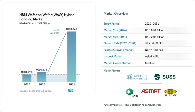
Mordor Intelligence에 의하면, HBM WoW(Wafer-on-Wafer) 하이브리드 본딩 시장 규모는 2025년에 3억 9,000만 달러로 평가되었고, 2031년까지 20억 6,000만 달러에 이를 것으로 예측되며, 2026-2031년 CAGR 32.21%로 성장할 전망입니다.
본 보고서는 본딩 아키텍처별(Wafer-To-Wafer 등), 본딩 유형별(구리 대 구리 등), 장비 유형별(웨이퍼 본더 등), 집적 수준별(2.5D 집적 등), 최종 사용자 산업별(반도체 파운드리 등), 용도별(메모리 및 스토리지 등), 그리고 지역별로 분류되어 있습니다. 시장 전망은 금액(달러) 기준으로 제시되어 있습니다.
세계의 HBM WoW(Wafer-on-Wafer) 하이브리드 본딩 시장 동향 및 인사이트
AI 가속기에서 HBM 스택 수 증가
AI 가속기의 로드맵에 따라 메모리 적층 수가 더욱 증가하고 있으며, 수직 방향의 상호 연결 밀도가 HBM WoW(Wafer-on-Wafer) 하이브리드 본딩 시장의 주요 성장 요인으로 작용하고 있습니다. SK하이닉스는 CES 2026에서 용량 48GB, 대역폭이 초당 2TB를 초과하는 16층 HBM4 디바이스를 발표했으며, 2026년 3분기 양산 개시를 목표로 하고 있습니다. Samsung Electronics는 자사의 1c DRAM 공정과 하이브리드 구리 본딩을 결합하여 HBM4의 동작 속도를 11.7Gb/s로 높였습니다고 발표했습니다. 이는 JEDEC의 기준치인 8Gb/s를 크게 상회하는 수치입니다. 『Electronics』에 게재된 동료 심사 리뷰에 따르면, 하이브리드 본딩을 통해 8층 HBM 구조에서 스택 전체의 두께가 15% 이상 감소했으며, 언더필을 직접 구리 연결로 대체함으로써 수직 방향의 열전달이 개선된 것으로 밝혀졌습니다. 적층 수가 12층을 초과하면 마이크로 범프만으로는 열기계적 응력이나 패키지 높이를 관리하기 어려워지므로, HBM WoW(Wafer-on-Wafer) 하이브리드 본딩 시장은 계속해서 차세대 AI 메모리 프로그램과 밀접한 관련을 맺고 있습니다.
로직과 메모리의 코패키지 통합
로직과 메모리를 단일 본딩 스택으로 통합함으로써, HBM WoW(Wafer-on-Wafer) 하이브리드 본딩 시장의 역할은 단순한 메모리 적층을 넘어 확대되고 있습니다. 홍콩과학기술대학교(HKUST)의 연구에 따르면, Wafer-on-Wafer(WoW) 방식으로 적층된 가속기는 NVIDIA A100의 기준치와 비교해 최대 7.17배 빠른 추론 성능을 발휘하는 반면, 치플릿 기반 설계는 모놀리식 방식에 비해 반복적인 엔지니어링 비용을 38.09% 절감했습니다. TSMC는 자사의 SoIC-X 플랫폼이 AMD의 2세대 3D V-Cache(9μm 피치)에 채택되어 기존 패키징에 비해 10배의 대역폭을 실현했다고 발표했습니다. Applied Materials는 Besi를 탑재한 자사의 Kinex 플랫폼이 Broadcom의 맞춤형 AI ASIC용으로 TSMC에서 이미 양산 중이며, 차세대 시스템에서는 50nm 이상의 정밀도와 더 높은 처리량을 목표로 하고 있다고 밝혔습니다. 이러한 성능과 비용 측면의 이점이 결합되어, 순수 HBM의 수주 주기가 변동하더라도 HBM WoW(Wafer-on-Wafer) 하이브리드 본딩 시장 수요는 유지될 전망입니다.
하이브리드 본딩 장비의 높은 자본 집약성
자본 집약성은 HBM WoW(Wafer-on-Wafer) 하이브리드 본딩 시장에 여전히 큰 걸림돌로 작용하고 있습니다. 이는 인증된 생산 라인을 구축하기 위해서는 본더 1대를 구입하는 것만으로는 불충분하기 때문입니다. Applied Materials는 하이브리드 본딩을 박막 형성, CMP, 공정 제어에 걸친 공정 체인으로 규정하고 있으며, 라인 인증을 위해서는 여러 범주에 걸친 고가의 장비가 필요함을 시사하고 있습니다. SUSS MicroTec사의 XBC300 Gen2 플랫폼은 웨이퍼 간 본딩, 일괄 다이-투-웨이퍼(Die-to-wafer), 순차적 다이-투-웨이퍼 기능을 하나의 시스템에 통합하고 있지만, 그 모듈성은 여전히 저비용 진입점이라기보다는 보다 광범위한 설비 투자 프로그램의 일환으로 자리 잡고 있습니다. 또한, 고객은 본더 주변에서 세정, 활성화, 계측, 어닐링 처리에 대한 지원도 필요로 하기 때문에 상용 수준의 수율을 달성하기까지 필요한 최소 투자액이 증가합니다. 이 때문에 HBM WoW(Wafer-on-Wafer) 하이브리드 본딩 시장의 도입은 자본력이 가장 풍부한 파운드리, 메모리 제조업체 및 첨단 패키징 업체를 중심으로 집중되고 있습니다.
부문 분석
2025년, HBM WoW(Wafer-on-Wafer) 하이브리드 본딩 시장에서 Wafer-To-Wafer 방식은 68.32%의 점유율을 차지했습니다. 이는 확립된 반도체 용도에서 해당 방식의 견실한 생산 실적과 높은 처리량을 반영한 것입니다. 이 아키텍처는 개별 다이를 배치하는 경우에 비해 사이클 타임이 훨씬 더 오래 걸리는 반면, 웨이퍼 전체를 몇 초 만에 본딩할 수 있기 때문에 HBM WoW(Wafer-on-Wafer) 하이브리드 본딩 시장에서 여전히 큰 비중을 차지하고 있습니다. 또한 3D NAND, CMOS 이미지 센서, DRAM에서의 실적이 높이 평가받고 있으며, 재현성 있는 제조 공정을 원하는 고객에게 도입 리스크를 낮출 수 있다는 점도 그 위상을 뒷받침하고 있습니다. 2026년 5월, imec과 EV Group은 GEMINI FB 시스템에서 300mm 웨이퍼 전체에 걸쳐 200nm 피치로 40nm 미만의 Cu 패드 오버레이 정밀도를 달성함으로써, 웨이퍼 간 본딩이 더욱 까다로운 로직 스태킹 작업에도 적용 가능함을 입증했습니다.
Die-to-wafer 시장은 2031년까지 연평균 성장률(CAGR) 32.68%를 나타낼 것으로 예측됩니다. 이는 치플릿(chiplet)이나 HBM 설계에서 전체 웨이퍼를 페어링하는 대신 선택적 배치가 필요한 경우가 많기 때문입니다. 이 접근 방식은 웨이퍼 크기에 차이가 있거나, 정상 작동이 확인된 웨이퍼를 다루는 것이 중요한 경우, 혹은 수율 관리 측면에서 풀 웨이퍼 본딩이 비효율적인 경우에 특히 효과적입니다. CEA-Leti는 ECTC 2026에서 1μm 피치의 기능적인 다이-투-웨이퍼(Die-to-wafer) 하이브리드 본딩을 시연하여, 고밀도 이종 AI 하드웨어의 중요한 기술적 병목 현상을 해소했습니다. 다이-투-다이(Die-to-die) 본딩은 HBM 웨이퍼-온-웨이퍼(WoW) 하이브리드 본딩 시장에서 여전히 규모가 작으며, 보다 선택적인 분야에 국한되어 있습니다. 이는 단일 다이의 매칭이 정당화되는 수율이 제한된 통합 사례에서 그 경제성이 가장 잘 발휘되기 때문입니다.
2025년에는 구리 대 구리 본딩이 시장 점유율의 55.06%를 차지했으며, 최첨단 메모리 및 로직 용도를 위한 HBM WoW(Wafer-on-Wafer) 하이브리드 본딩 시장의 표준 공정이 되었습니다. 소니, 삼성, TSMC, SK하이닉스, 도쿄 일렉트론의 구현 사례에 대한 IEEE 조사에 따르면, 직접 Cu-Cu 본딩이 10μm 미만의 피치를 지원하면서도 범프 기반 대체 기법보다 우수한 열적 및 전기적 성능을 발휘하는 것으로 확인되었습니다. 이러한 성능상의 우위는 HBM 및 적층 로직에서 중요합니다. 층 수가 늘어날수록 상호 연결 밀도와 열 전달 관리가 어려워지기 때문입니다. 구리-패드 간 및 금속-패드 간 본딩 기법은 기존의 플립칩에서 보다 진보된 본딩 공정으로 전환하는 고객들에게 계속해서 과도기적인 선택지로 기능하고 있습니다.
산화물 대 산화물 및 금속 대 산화물 하이브리드 본딩 시장은 2031년까지 연평균 성장률(CAGR) 32.61%를 나타낼 것으로 예측되며, 이는 유전체 호환성이 필수적인 포토닉스 및 센서 통합에 대한 관심이 높아지고 있음을 반영합니다. TSMC의 SoIC-X는 Cu 패드와 최적화된 SiCN 유전체를 채택하고 있으며, imec의 200nm 피치 실증 실험에서도 최적화된 CMP 공정을 갖춘 SiCN이 사용되었습니다. 이는 유전체 엔지니어링이 이미 양산 수준의 미세화의 일부가 되었음을 보여줍니다. 이에 따라 본딩 방식의 개발은 본딩 형성 자체보다 표면 처리, CMP 균일성 및 오버레이 제어와 밀접하게 연관되어 있습니다. 더 많은 이종 디바이스가 HBM WoW(Wafer-on-Wafer) 하이브리드 본딩 시장에 진입함에 따라, 단순한 구리 인터페이스와 완전한 재료 스택 간의 격차는 점점 더 좁혀질 것입니다.
지역별 분석
2025년에는 아시아태평양이 83.61%의 점유율을 차지하며, HBM WoW(Wafer-on-Wafer) 하이브리드 본딩 시장의 중심지로서 확고한 입지를 다지고 있습니다. 이 지역이 주도적인 위치를 차지하는 이유는 한국에 Samsung Electronics(Samsung Electronics)와 SK하이닉스(SK hynix)가 거점을 두고 있고, 대만에는 TSMC의 SoIC 플랫폼이 있으며, 일본이 여전히 장비 개발 및 소재 공급의 주요 거점이기 때문입니다. 이러한 집중 현상으로 인해 HBM WoW(Wafer-on-Wafer) 하이브리드 본딩 시장은 이미 첨단 노드 규모로 사업을 전개하고 있는 메모리 제조업체, 파운드리, 벤더로 구성된 제한된 그룹과 밀접하게 연결되어 있습니다. Tokyo Electron은 2025년 10월, 규슈에 새로운 첨단 패키징 장비 개발 거점을 건설하기 위해 3억 3,000만 달러를 투자한다고 발표했습니다(계산에는 2025년 평균 환율을 사용). 중국도 본딩 관련 장비의 국내 대체품 개발을 추진하고 있으며, 이는 수출 규제가 공급망을 재편하고 현지 기술 개발을 촉진하고 있음을 반영합니다.
북미는 2031년까지 연평균 성장률(CAGR) 33.02%를 나타낼 것으로 예측되며, 그 결과 해당 지역의 HBM WoW(Wafer-on-Wafer) 하이브리드 본딩 시장 규모는 다른 어떤 지역보다 빠르게 확대될 전망입니다. 그 주된 요인은 ‘CHIPS 법’에 힘입은 첨단 패키징 및 국내 반도체 제조에 대한 투자입니다. 인텔은 애리조나주, 뉴멕시코주, 오하이오주, 오리건주의 거점을 지원하기 위해 78억 6,000만 달러 규모의 ‘CHIPS 법’ 자금 지원을 확정했습니다. 여기에는 Foveros Direct 하이브리드 본딩과 관련된 프로그램도 포함되어 있습니다. TSMC의 애리조나주 확장도 이 지역의 중요성을 뒷받침하고 있습니다. AI 관련 고객들이 국내 공급망 내에서 첨단 패키징 역량을 점점 더 요구하고 있기 때문입니다. 유럽의 점유율은 여전히 작지만, 벨기에의 imec, 독일의 SUSS MicroTec, 네덜란드의 Besi, 프랑스의 CEA-Leti를 통해 전략적으로 중요한 위치를 계속 차지하고 있습니다.
남미, 중동 및 아프리카는 이러한 유형의 장비를 지원할 수 있는 최첨단 반도체 제조 인프라가 부족하기 때문에 2025년 시점에서는 극히 미미한 점유율에 그칠 것으로 보입니다. HBM WoW(Wafer-on-Wafer) 하이브리드 본딩 시장에서 이들 지역의 역할은 주요 생산이나 연구 활동이라기보다는 서비스 제공 및 유통 지원에 국한될 가능성이 높습니다. 즉, 2026-2031년 기간 동안 이 지역들로부터 의미 있는 투자 수요는 나타나지 않을 것으로 예측됩니다.
기타 혜택 :
- 엑셀 형식 시장 예측(ME) 시트
- 3개월간의 애널리스트 지원
자주 묻는 질문
목차
제1장 서론
제2장 조사 방법
제3장 주요 요약
제4장 시장 구도
제5장 시장 규모 및 성장 예측
제6장 경쟁 구도
제7장 시장 기회 및 향후 전망
AJY 26.08.11According to Mordor Intelligence, the HBM wafer-on-Wafer (wow) hybrid bonding market size stood at USD 0.39 billion in 2025 and is forecast to reach USD 2.06 billion by 2031, growing at a CAGR of 32.21% over 2026-2031.
This report is Segmented by Bonding Architecture (Wafer-To-Wafer, and More), Bonding Type (Copper-To-Copper, and More), Equipment Type (Wafer Bonders, and More), Integration Level (2. 5D Integration, and More), End-User Industry (Semiconductor Foundries, and More), Application (Memory and Storage, and More), and Geography. The Market Forecasts are Provided in Terms of Value (USD).
Global HBM Wafer-on-Wafer (WoW) Hybrid Bonding Market Trends and Insights
Rising HBM Stack Counts in AI Accelerators
AI accelerator roadmaps are pushing memory stack counts higher, making vertical interconnect density a central growth driver for the HBM Wafer-on-Wafer (WoW) hybrid bonding market. SK hynix unveiled a 16-layer HBM4 device with 48GB capacity and bandwidth above 2TB per second at CES 2026, and the company targeted mass production in the third quarter of 2026. Samsung disclosed HBM4 operating speeds of 11.7Gb/s by combining its 1c DRAM process with hybrid copper bonding, which placed it well above the JEDEC baseline of 8Gb/s. A peer-reviewed review in Electronics found that hybrid bonding reduced total stack height by more than 15% in an 8-layer HBM structure and improved vertical heat transfer by replacing underfill with direct copper connections. As stack counts exceed 12 layers, thermomechanical stress and package height become harder to manage with microbumps alone, so the HBM Wafer-on-Wafer (WoW) hybrid bonding market remains closely linked to next-generation AI memory programs.
Co-Packaged Logic and Memory Integration
Co-integrating logic and memory in a single bonded stack is expanding the role of the HBM Wafer-on-Wafer (WoW) hybrid bonding market beyond pure memory stacking. HKUST research showed that wafer-on-wafer stacked accelerators delivered inference up to 7.17 times faster than an NVIDIA A100 baseline, while chiplet-based designs reduced recurring engineering costs by 38.09% compared with monolithic alternatives. TSMC stated that its SoIC-X platform was used in AMD's second-generation 3D V-Cache at 9µm pitch and delivered 10 times the bandwidth of conventional packaging. Applied Materials said its Kinex platform with Besi is already in mass production at TSMC for Broadcom custom AI ASICs, and the next-generation system targets 50nm accuracy or better with higher throughput. This combination of performance and cost benefits means the HBM Wafer-on-Wafer (WoW) hybrid bonding market can sustain demand even when pure HBM order cycles fluctuate.
High Capital Intensity of Hybrid Bonding Tooling
Capital intensity remains a real brake on the HBM Wafer-on-Wafer (WoW) hybrid bonding market because qualified production lines require more than a single bonder purchase. Applied Materials positioned hybrid bonding as a process chain spanning deposition, CMP, and process control, indicating that line qualification requires multiple categories of high-value equipment. SUSS MicroTec's XBC300 Gen2 platform combines wafer-to-wafer, collective die-to-wafer, and sequential die-to-wafer capability in one system, but that modularity still sits within a broader capital program rather than a low-cost entry point. Customers also need cleaning, activation, metrology, and annealing support around the bonder, which increases the minimum spend required before commercial yields can be achieved. This keeps adoption concentrated among the most capitalized foundries, memory makers, and advanced packaging operators in the HBM Wafer-on-Wafer (WoW) hybrid bonding market.
Other drivers and restraints analyzed in the detailed report include:
- Sub-10 Micron Interconnect Pitch Migration
- Front-End Wafer-Level Process Control Adoption
- Yield Sensitivity to Particle and Surface Defects
For complete list of drivers and restraints, kindly check the Table Of Contents.
Segment Analysis
Wafer-to-wafer held 68.32% of the HBM Wafer-on-Wafer (WoW) hybrid bonding market share in 2025, reflecting its strong production record and higher throughput in established semiconductor applications. The architecture remained the larger part of the HBM Wafer-on-Wafer (WoW) hybrid bonding market because it can bond an entire wafer in seconds rather than placing individual dies over much longer cycle times. Its position was also supported by proven use in 3D NAND, CMOS image sensors, and DRAM, thereby reducing adoption risk for customers seeking a repeatable manufacturing route. In May 2026, imec and EV Group demonstrated less than 40nm Cu pad overlay accuracy across a full 300mm wafer at a 200nm pitch on the GEMINI FB system, demonstrating that wafer-to-wafer bonding can move into much more demanding logic stacking work.
Die-to-wafer is projected to grow at a 32.68% CAGR through 2031 because chiplet and HBM designs often need selective placement rather than full-wafer pairing. The approach is especially relevant when die sizes differ, when handling known-good dies matters, or when yield management makes full-wafer bonding inefficient. CEA-Leti demonstrated functional die-to-wafer hybrid bonding at a 1µm pitch at ECTC 2026, removing a key technical bottleneck for high-density heterogeneous AI hardware. Die-to-die bonding remained a smaller and more selective part of the HBM Wafer-on-Wafer (WoW) hybrid bonding market because its economics work best in limited-yield integration cases where single-die matching is justified.
Copper-to-Copper bonding captured 55.06% of the market share in 2025, making it the reference process in the HBM Wafer-on-Wafer (WoW) hybrid bonding market for leading-edge memory and logic applications. An IEEE research review of implementations across Sony, Samsung, TSMC, SK hynix, and Tokyo Electron confirmed that direct Cu-Cu bonding supports pitches below 10µm while offering stronger thermal and electrical performance than bump-based alternatives. That performance advantage matters in HBM and stacked logic because both interconnect density and heat transfer become harder to manage as layer counts increase. Copper-to-pad and metal-to-pad routes continue to serve as transitional options for customers moving from conventional flip-chip to more advanced bonding flows.
Oxide-to-Oxide and Metal-Oxide Hybrid Bonding is projected to grow at a 32.61% CAGR through 2031, reflecting rising interest in photonics and sensor integration, where dielectric compatibility is essential. TSMC's SoIC-X uses an optimized SiCN dielectric with Cu pads, and imec's 200nm pitch demonstration also used SiCN with an optimized CMP flow, demonstrating that dielectric engineering is already part of production-grade scaling. This keeps bonding type development tightly linked to surface preparation, CMP uniformity, and overlay control rather than to bond formation alone. As more heterogeneous devices move into the HBM Wafer-on-Wafer (WoW) hybrid bonding market, the gap between a simple copper interface and a full materials stack will keep narrowing.
Complete Report Scope:
- By Bonding Architecture
- Wafer-to-Wafer
- Die-to-Wafer
- Die-to-Die
- By Bonding Type
- Copper-to-Copper
- Copper-to-Pad and Metal-to-Pad
- Oxide-to-Oxide and Metal-Oxide Hybrid Bonding
- By Equipment Type
- Wafer Bonders
- Surface Preparation Tools
- Inspection and Metrology Tools
- Cleaning and CMP Systems
- By Integration Level
- 2.5D Integration
- 3D Integration
- Chiplet Integration
- By End User Industry
- Semiconductor Foundries
- OSATs
- Integrated Device Manufacturers
- Other End-user Industries
- By Application
- Memory and Storage
- Computing and Logic
- Sensing and Interface
- Connectivity and Communications
- Photonics and Optical Interconnects
- By Geography
- North America
- United States
- Canada
- Mexico
- Europe
- Germany
- United Kingdom
- France
- Italy
- Rest of Europe
- Asia-Pacific
- China
- Japan
- South Korea
- Taiwan
- India
- Rest of Asia-Pacific
- South America
- Middle East and Africa
- North America
Geography Analysis
Asia-Pacific held an 83.61% share in 2025, making it the clear center of the HBM Wafer-on-Wafer (WoW) hybrid bonding market. The region leads because South Korea houses Samsung Electronics and SK hynix, Taiwan hosts TSMC's SoIC platform, and Japan remains a major base for equipment development and materials supply. This concentration keeps the HBM Wafer-on-Wafer (WoW) hybrid bonding market closely tied to a compact group of memory manufacturers, foundries, and equipment vendors that already operate at advanced-node scale. Tokyo Electron announced a USD 330 million investment in October 2025 to build a new advanced packaging equipment development hub in Kyushu, at the 2025 average exchange rate used as input. China is also building domestic alternatives in bonding-related equipment, which reflects how export controls are reshaping the supply chain and encouraging local capability development.
North America is projected to post a 33.02% CAGR through 2031, and its HBM Wafer-on-Wafer (WoW) hybrid bonding market size is therefore set to expand faster than any other region. The main driver is the CHIPS Act-backed investment in advanced packaging and domestic semiconductor manufacturing. Intel finalized a USD 7.86 billion CHIPS Act funding award to support sites in Arizona, New Mexico, Ohio, and Oregon, including programs tied to Foveros Direct hybrid bonding. TSMC's Arizona expansion also supports the regional case because AI customers increasingly want advanced packaging capacity inside a domestic supply chain. Europe remains smaller in share, but it stays strategically relevant through imec in Belgium, SUSS MicroTec in Germany, Besi in the Netherlands, and CEA-Leti in France.
South America and the Middle East and Africa held only a negligible position in 2025 because they lack leading-edge semiconductor manufacturing infrastructure for this equipment class. Their role in the HBM Wafer-on-Wafer (WoW) hybrid bonding market is more likely to stay limited to service coverage and distribution support than to primary production or research activity. This means meaningful investment demand from these regions is not expected to emerge within the 2026-2031 period.
- EV Group
- Applied Materials, Inc.
- SUSS MicroTec SE
- BE Semiconductor Industries N.V.
- ASMPT Limited
- Tokyo Electron Limited
- KLA Corporation
- Onto Innovation Inc.
- Lam Research Corporation
- DISCO Corporation
- SHIBAURA MECHATRONICS CORPORATION
- Hanmi Semiconductor Co., Ltd.
- Toray Engineering Co., Ltd.
- BEIJING U-PRECISION TECH CO., LTD.
- Applied Microengineering Ltd.
- SET Corporation SA
- Piotech, Inc.
- NAURA Technology Group Co., Ltd.
- Nidec Machine Tool Corporation
Additional Benefits:
- The market estimate (ME) sheet in Excel format
- 3 months of analyst support
TABLE OF CONTENTS
1 INTRODUCTION
- 1.1 Study Assumptions and Market Definition
- 1.2 Scope of the Study
2 RESEARCH METHODOLOGY
3 EXECUTIVE SUMMARY
4 MARKET LANDSCAPE
- 4.1 Market Overview
- 4.2 Market Drivers
- 4.2.1 Rising HBM Stack Counts in AI Accelerators
- 4.2.2 Co-Packaged Logic and Memory Integration
- 4.2.3 Sub-10 Micron Interconnect Pitch Migration
- 4.2.4 Front-End Wafer-Level Process Control Adoption
- 4.2.5 Pilot-Line De-Risking for Chiplet-Based HBM Architectures
- 4.2.6 Photonics and Sensor Co-Integration Demand
- 4.3 Market Restraints
- 4.3.1 High Capital Intensity of Hybrid Bonding Tooling
- 4.3.2 Yield Sensitivity to Particle and Surface Defects
- 4.3.3 Limited Qualified Supplier Base for Ultra-Precision Bonding
- 4.3.4 Thermo-Mechanical Stress Risks in Ultra-Thin Stacked Dies
- 4.4 Industry Value Chain Analysis
- 4.5 Regulatory Landscape
- 4.6 Technological Outlook
- 4.7 Porter's Five Forces Analysis
- 4.7.1 Bargaining Power of Suppliers
- 4.7.2 Bargaining Power of Buyers
- 4.7.3 Threat of New Entrants
- 4.7.4 Threat of Substitutes
- 4.7.5 Intensity of Competitive Rivalry
- 4.8 Impact of Macroeconomic Factors on the Market
5 MARKET SIZE AND GROWTH FORECASTS (VALUE)
- 5.1 By Bonding Architecture
- 5.1.1 Wafer-to-Wafer
- 5.1.2 Die-to-Wafer
- 5.1.3 Die-to-Die
- 5.2 By Bonding Type
- 5.2.1 Copper-to-Copper
- 5.2.2 Copper-to-Pad and Metal-to-Pad
- 5.2.3 Oxide-to-Oxide and Metal-Oxide Hybrid Bonding
- 5.3 By Equipment Type
- 5.3.1 Wafer Bonders
- 5.3.2 Surface Preparation Tools
- 5.3.3 Inspection and Metrology Tools
- 5.3.4 Cleaning and CMP Systems
- 5.4 By Integration Level
- 5.4.1 2.5D Integration
- 5.4.2 3D Integration
- 5.4.3 Chiplet Integration
- 5.5 By End User Industry
- 5.5.1 Semiconductor Foundries
- 5.5.2 OSATs
- 5.5.3 Integrated Device Manufacturers
- 5.5.4 Other End-user Industries
- 5.6 By Application
- 5.6.1 Memory and Storage
- 5.6.2 Computing and Logic
- 5.6.3 Sensing and Interface
- 5.6.4 Connectivity and Communications
- 5.6.5 Photonics and Optical Interconnects
- 5.7 By Geography
- 5.7.1 North America
- 5.7.1.1 United States
- 5.7.1.2 Canada
- 5.7.1.3 Mexico
- 5.7.2 Europe
- 5.7.2.1 Germany
- 5.7.2.2 United Kingdom
- 5.7.2.3 France
- 5.7.2.4 Italy
- 5.7.2.5 Rest of Europe
- 5.7.3 Asia-Pacific
- 5.7.3.1 China
- 5.7.3.2 Japan
- 5.7.3.3 South Korea
- 5.7.3.4 Taiwan
- 5.7.3.5 India
- 5.7.3.6 Rest of Asia-Pacific
- 5.7.4 South America
- 5.7.5 Middle East and Africa
- 5.7.1 North America
6 COMPETITIVE LANDSCAPE
- 6.1 Market Concentration
- 6.2 Strategic Moves
- 6.3 Market Share Analysis
- 6.4 Company Profiles (includes Global Level Overview, Market Level Overview, Core Segments, Financials as available, Strategic Information, Market Rank/Share, Products and Services, Recent Developments)
- 6.4.1 EV Group
- 6.4.2 Applied Materials, Inc.
- 6.4.3 SUSS MicroTec SE
- 6.4.4 BE Semiconductor Industries N.V.
- 6.4.5 ASMPT Limited
- 6.4.6 Tokyo Electron Limited
- 6.4.7 KLA Corporation
- 6.4.8 Onto Innovation Inc.
- 6.4.9 Lam Research Corporation
- 6.4.10 DISCO Corporation
- 6.4.11 SHIBAURA MECHATRONICS CORPORATION
- 6.4.12 Hanmi Semiconductor Co., Ltd.
- 6.4.13 Toray Engineering Co., Ltd.
- 6.4.14 BEIJING U-PRECISION TECH CO., LTD.
- 6.4.15 Applied Microengineering Ltd.
- 6.4.16 SET Corporation SA
- 6.4.17 Piotech, Inc.
- 6.4.18 NAURA Technology Group Co., Ltd.
- 6.4.19 Nidec Machine Tool Corporation
7 MARKET OPPORTUNITIES AND FUTURE OUTLOOK
- 7.1 White-Space and Unmet-Need Assessment


