

|
시장보고서
상품코드
2113965
하이브리드 광집적회로 : 시장 점유율 분석, 업계 동향 및 통계, 성장 예측(2026-2031년)Hybrid Photonic Integrated Circuit - Market Share Analysis, Industry Trends & Statistics, Growth Forecasts (2026 - 2031) |
||||||
 Mordor Intelligence
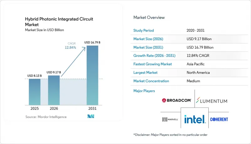
Mordor Intelligence에 의하면, 하이브리드 광집적회로 시장 규모는 2025년 81억 3,000만 달러로 평가되었습니다. 2026년에는 91억 7,000만 달러로 확대되어 2026년부터 2031년에 걸쳐 CAGR 12.84%로 성장을 지속하여, 2031년에는 167억 9,000만 달러에 이를 것으로 예측됩니다.
본 보고서는 용도별(데이터 통신 및 클라우드 상호 연결, 통신 전송 및 5G/6G 모바일 백홀 등), 소재 플랫폼별(실리콘-III-V 하이브리드, 실리콘 질화물-III-V 등),최종 사용자 산업별(클라우드 서비스 제공업체, 통신 사업자 및 네트워크 OEM 등), 그리고 지역별로 분류되어 있습니다. 시장 예측은 금액(달러) 기준으로 제시되어 있습니다.
세계의 하이브리드 광집적회로 시장 동향 및 인사이트
AI/ML에 최적화된 코패키지드 옵틱스 수요
현재, 1조 파라미터 규모의 모델 훈련으로 인해 랙당 트래픽은 초당 400테라비트를 초과하고 있습니다. 이는 프론트 패널 플러그인 방식으로는 허용할 수 없는 수준의 전력 손실 없이 달성할 수 없는 임계값입니다. 코패키지드 옵틱스의 경우, 포토닉 다이를 스위치 ASIC 옆에 배치함으로써 전기적 도달 거리를 단축하고 홉 지연을 10나노초 미만으로 억제하고 있습니다. Meta는 2024년 Grand Teton 클러스터에서 양산 준비가 완료되었음을 입증했으며, Ayar Labs는 1만 개 이상의 광 칩렛을 출하하여 2025년 양산 확대를 확보했습니다. 유럽과 인도의 ‘Sovereign-AI’ 규제에서는 로컬 추론이 의무화되어 있어, 이에 따라 소형 광 I/O가 필요한 중규모 도입이 촉진되고 있습니다. 조기 도입 기업들로부터는 개별 광 디바이스에 비해 상호 연결 전력이 30% 감소하고 투자 회수 기간이 2년 단축되었습니다는 보고가 있어, 이에 따라 하이브리드 광 집적 회로 시장의 보급 곡선이 가속화되고 있습니다.
하이퍼스케일 데이터센터의 대역폭 폭발적 증가
동영상 스트리밍 및 생성형 AI의 보급을 배경으로, 2026년에는 전 세계 IP 트래픽이 4.8 제타바이트에 달할 것으로 예측됩니다. 각 하이퍼스케일러 기업들은 2025년에 800기가비트 이더넷 스파인으로, 2026년에는 1.6테라비트 광통신으로 전환할 것으로 예상되며, 이에 따라 리프레시 주기가 5년에서 3년으로 단축될 전망입니다. 마이크로소프트는 2024년에 백본의 60%를 400기가비트 코히런트 통신으로 업그레이드하여 비트당 비용을 35% 절감했습니다. 속도가 향상될 때마다 링크 버짓이 엄격해지고, 모놀리식 광전자 공동 설계가 유리해짐에 따라 하이브리드 광집적회로 시장 수요가 증가하고 있습니다. 박막 리튬 니오브산염은 인듐 인화물보다 3데시벨 더 높은 효율을 실현하여 저전압 1.6테라비트 모듈을 가능하게 합니다.
이종 본딩의 수율 문제
300mm 실리콘 위에 III-V족 다이를 본딩하는 경우, 수율은 여전히 92-95%에 머물러 있으며, 수율이 1포인트 하락할 때마다 단위 비용이 3-5% 상승하고 있습니다. 타워 세미컨덕터(Tower Semiconductor)는 2024년 4분기에 수율을 94%까지 개선했으나, 자동차 등급 목표인 98%에는 아직 도달하지 못했습니다. 열 어닐링 중 발생하는 보이드 형성은 최대 2데시벨의 광 손실을 초래하고, 층간 박리를 가속화합니다. Imec의 플라즈마 활성화 본딩은 보이드를 70% 감소시키지만, 그 대신 공정 비용을 15% 상승시킵니다. 인증된 파운드리 업체가 5곳에 그치고 있는 점이 단기적인 공급 상한선으로 작용하고 있으며, 새로운 생산 능력이 확보되기 전까지는 하이브리드 광집적회로 시장의 확대를 억제하게 될 것입니다.
부문 분석
고성능 컴퓨팅(HPC) 및 AI 가속기는 전기식 SerDes를 능가하는 GPU 간 대역폭의 급증에 힘입어 가장 높은 연평균 성장률(CAGR) 13.98%로 성장을 지속하고 있습니다. 데이터 통신 및 클라우드 상호 연결은 100기가비트 및 400기가비트 링크의 기존 도입 기반이 800기가비트 광통신으로 전환되고 있는 것을 배경으로, 46.05%로 여전히 가장 큰 점유율을 차지하고 있습니다. AI 가속기용 하이브리드 광집적회로 시장 규모는 유럽 및 아시아의 국가 주도의 AI 인프라 구축을 원동력으로 2026년부터 2031년 사이에 24억 5,000만 달러 이상으로 확대될 것으로 예측됩니다. 통신 백홀, LiDAR 센싱, RF 포토닉스는 특수한 성능 요구 사항이 있어 틈새 시장이지만 수익성이 높은 위치를 유지하고 있습니다.
중앙 집중형 트레이닝 클러스터에서 엣지 추론으로의 전환에 따라, 광 I/O는 서버, 스마트 NIC, 나아가 임베디드 시스템으로까지 보급이 확대되고 있습니다. Meta사의 코패키징 방식 도입으로 랙 내 지연 시간은 10나노초 미만으로 단축되었습니다. 자동차용 LiDAR는 단일 다이 위에 파장 가변 레이저와 코히런트 수신기를 통합한 1550나노미터 FMCW 설계로 전환되고 있으며, 하이브리드 방식의 채택이 더욱 확대되고 있습니다. RF 포토닉스는 차세대 레이더를 위해 40기가헤르츠의 순간 대역폭을 지원하며, 방위 분야 수요를 충족시키고 있습니다. 의료 진단 분야에서는 실시간 병원체 검출을 목적으로 한 랩-온-칩 포토닉스를 활용한 초기 임상시험이 시작되었습니다.
지역별 분석
북미는 인텔의 뉴멕시코주 팹 및 Ayar Labs의 양산 출하에 힘입어 2025년 매출의 38.10%를 차지했습니다. 연방 CHIPS법에 따른 총 15억 달러의 보조금은 포토닉스 연구개발에 투입되어 이 지역의 선도적 지위를 공고히 하고 있습니다. 미국의 클라우드 사업자들은 800기가비트 스파인 네트워크 도입을 가속화하고 있어, 국내 팹에 막대한 수요를 불러오고 있습니다. 캐나다의 양자 포토닉스 프로그램으로 인해 실리콘 질화물 도파관용 맞춤형 주문이 증가하고 있습니다.
아시아태평양은 중국의 100억 달러 규모 파운드리 지원 정책과 대만의 첨단 패키징 클러스터를 원동력으로 13.55%라는 최고 연평균 성장률(CAGR)을 기록하고 있습니다. TSMC의 마츠에 파일럿 라인은 하이브리드 다이 생산을 시작할 예정이며, 2026년까지월1만 웨이퍼 생산을 목표로 하고 있습니다. 일본의 2억 달러 규모 포토닉스 컨소시엄에서는 후지쯔와 NTT가 1.6테라비트 코히런트 시스템 개발을 위해 제휴하고 있는 반면, 인도의 ‘반도체 미션’은 국내 팹에 5억 달러를 배정하고 있습니다. 동남아시아의 EMS 벤더들은 소비자용 광학 부품을 위한 폴리머 포토닉스에 주목하며, 지역 내 공급망을 확대되고 있습니다.
유럽은 Imec의 멀티프로젝트 웨이퍼 프로그램과 네덜란드의 리소그래피 생태계로부터 혜택을 받고 있지만, 하이브리드 광집적회로 시장 규모는 북미 및 아시아태평양에 뒤처져 있습니다. 유럽의 ‘칩스 법(Chips Act)’에서는 이종 접합 및 양자 소자에 초점을 맞춘 파일럿 라인에 5억 유로가 배정되었습니다. 독일과 프랑스는 자동차용 LiDAR에 대한 자금 지원을 주도하고 있는 반면, 영국은 바이오센싱용 실리콘 포토닉스를 지원하고 있습니다. STC 등 중동의 통신 사업자들은 메트로링크용 400기가비트 코히런트 시스템을 도입하고 있지만, 현지 생산은 여전히 극히 미미한 수준입니다. 남아프리카공화국에서 진행 중인 아프리카 초기 시범 프로젝트에서는 광대역 접속용 실리콘 포토닉스가 검토되고 있으며, 향후 보급을 위한 기반이 마련되고 있습니다.
기타 혜택 :
- 엑셀 형식 시장 예측(ME) 시트
- 3개월간의 애널리스트 지원
자주 묻는 질문
목차
제1장 서론
제2장 조사 방법
제3장 주요 요약
제4장 시장 구도
제5장 시장 규모 및 성장 예측
제6장 경쟁 구도
제7장 시장 기회 및 향후 전망
KTH 26.08.26According to Mordor Intelligence, the hybrid photonic integrated circuit market size is expected to grow from USD 8.13 billion in 2025 to USD 9.17 billion in 2026 and is forecast to reach USD 16.79 billion by 2031 at 12.84% CAGR over 2026-2031.
This report is Segmented by Application (Datacom and Cloud Interconnect, Telecom Transport and 5G/6G Mobile Backhaul, and More), Material Platform (Silicon-III-V Hybrid, Silicon Nitride-III-V, and More), End-User Industry (Cloud Service Providers, Telecom Operators and Network OEMs, and More), and Geography. The Market Forecasts are Provided in Terms of Value (USD).
Global Hybrid Photonic Integrated Circuit Market Trends and Insights
AI/ML-Optimised Co-Packaged Optics Demand
Training trillion-parameter models now drives per-rack traffic beyond 400 terabits per second, a threshold that front-panel pluggables cannot meet without prohibitive power loss. Co-packaged optics place photonic dies beside switch ASICs, trimming electrical reach and delivering sub-10-nanosecond hop latency. Meta validated production readiness in its 2024 Grand Teton cluster, while Ayar Labs shipped more than 10,000 optical chiplets and secured 2025 volume ramps. Sovereign-AI rules in Europe and India require local inference, driving mid-scale deployments that necessitate compact optical I/O. Early adopters report a 30% lower interconnect power and a 2-year payback period versus discrete optics, thereby accelerating the adoption curve of the hybrid photonic integrated circuit market.
Hyperscale Datacenter Bandwidth Explosion
Global IP traffic is projected to reach 4.8 zettabytes in 2026, driven by video streaming and the adoption of generative AI. Hyperscalers are expected to transition to 800 gigabit Ethernet spines in 2025 and 1.6 terabit optics in 2026, thereby compressing refresh cycles from 5 years to 3 years. Microsoft upgraded 60% of its backbone to 400 gigabit coherent in 2024, cutting cost per bit by 35%. Each speed jump tightens the link budget and favors monolithic photonic-electronic co-design, thereby boosting demand for the hybrid photonic integrated circuit market. Thin-film lithium niobate offers 3 decibels higher efficiency than indium phosphide, enabling lower-voltage 1.6 terabit modules.
Heterogeneous Bonding Yield Challenges
Bonding III-V dies on 300 millimeter silicon still reaches only 92 to 95% yield, pushing up unit cost by 3-5% per lost point. Tower Semiconductor improved to 94% in Q4 2024 but remains shy of the 98% goal for automotive grade. Void formation during thermal anneal adds up to 2 decibel optical loss and accelerates delamination. Imec's plasma-activated bonding lowers voids by 70% yet raises process cost by 15%. The limited pool of five qualified foundries acts as a near-term supply cap and restrains the hybrid photonic integrated circuit market until new capacity matures.
Other drivers and restraints analyzed in the detailed report include:
- 5G/6G Fronthaul and Mid-Haul Optical Densification
- Silicon + III-V Heterointegration Cost Crossover
- Thermal Mismatch Reliability Issues
For complete list of drivers and restraints, kindly check the Table Of Contents.
Segment Analysis
High-Performance Computing and AI Accelerators account for the fastest 13.98% CAGR, reflecting surging inter-GPU bandwidth that outstrips electrical SerDes. Datacom and Cloud Interconnect remains the largest slice with 46.05%, supported by the installed base of 100 and 400 gigabit links that migrate to 800 gigabit optics. The hybrid photonic integrated circuit market size for AI accelerators is projected to add more than USD 2.45 billion between 2026 and 2031, driven by sovereign-AI buildouts in Europe and Asia. Telecom backhaul, LiDAR sensing, and RF-photonics retain niche but profitable positions thanks to specialized performance needs.
The shift from centralized training clusters to edge inference pushes optical I/O into servers, smart NICs, and even embedded systems. Meta's co-packaged deployment cut intra-rack latency under 10 nanoseconds. Automotive LiDAR is moving to 1550-nanometer FMCW designs that integrate tunable lasers and coherent receivers on a single die, reinforcing hybrid adoption. RF-photonics supports a 40-gigahertz instantaneous bandwidth for next-generation radar, meeting defense demand. Healthcare diagnostics enter early trials with lab-on-chip photonics for real-time pathogen detection.
Complete Report Scope:
- By Application
- Datacom and Cloud Interconnect
- Telecom Transport and 5G/6G Mobile Backhaul
- LiDAR and Optical Sensing
- High-performance Computing (HPC) and AI Accelerators
- RF-Photonics and Microwave Photonics
- By Material Platform
- Silicon-III-V Hybrid (InP/GaAs on Si)
- Silicon Nitride-III-V
- Polymer Photonics Hybrid
- Thin-film Lithium Niobate on Si
- Others (SiGe, AlN, etc.)
- By End-user Industry
- Cloud Service Providers (Hyperscalers)
- Telecom Operators and Network OEMs
- Defense and Aerospace
- Healthcare and Biosensing OEMs
- Industrial and Automotive OEMs
- By Geography
- North America
- United States
- Canada
- Mexico
- Europe
- Germany
- United Kingdom
- France
- Netherlands
- Rest of Europe
- Asia-Pacific
- China
- India
- Japan
- South Korea
- ASEAN
- Rest of Asia-Pacific
- Rest of the World
- North America
Geography Analysis
North America held 38.10% of 2025 revenue, buoyed by Intel's New Mexico fab and Ayar Labs volume shipments. The Federal CHIPS Act grants, totaling USD 1.5 billion, earmark photonics R&D, ensuring local leadership. Cloud builders in the United States fast-track 800 gigabit spines, pulling high-volume demand into domestic fabs. Canada's quantum photonics programs add specialty orders for silicon nitride waveguides.
Asia-Pacific posts the highest 13.55% CAGR, driven by China's USD 10 billion foundry stimulus and Taiwan's advanced packaging clusters. TSMC's Songjiang pilot line is set to begin hybrid die runs, targeting 10,000 wafers per month by 2026. Japan's USD 200 million photonics consortium teams Fujitsu and NTT on a 1.6 terabit coherent system, while India's Semiconductor Mission allocates USD 500 million for local fabs. South-East Asian EMS vendors eye polymer photonics for consumer optics, extending regional supply chains.
Europe benefits from Imec's multi-project wafer program and the Netherlands' lithography ecosystem; however, its hybrid photonic integrated circuit market size lags behind that of North America and the Asia-Pacific region. The European Chips Act reserves EUR 500 million for pilot lines focused on heterogeneous bonding and quantum devices. Germany and France direct automotive LiDAR funding, while the U.K. backs silicon photonics for biosensing. Middle East operators like STC install 400 gigabit coherent for metro links, though local manufacturing remains minimal. Africa's early pilots in South Africa explore silicon photonics for broadband access, setting a foundation for future uptake.
- Intel Corporation
- Cisco Systems (Acacia Communications)
- Broadcom Inc.
- Marvell Technology (Inphi)
- Lumentum Holdings
- Coherent Corp. (II-VI)
- Rockley Photonics
- Ayar Labs
- Nokia (Bell Labs)
- Fujitsu Optical Components
- NeoPhotonics (Lumentum)
- Ciena Corporation
- Effect Photonics
- POET Technologies
- Ligentec SA
- Infinera Corporation
- Hewlett Packard Enterprise (HPC interconnect)
- GlobalFoundries (SiPh services)
- Imec (foundry and MPW)
- Tower Semiconductor
Additional Benefits:
- The market estimate (ME) sheet in Excel format
- 3 months of analyst support
TABLE OF CONTENTS
1 INTRODUCTION
- 1.1 Study Assumptions and Market Definition
- 1.2 Scope of the Study
2 RESEARCH METHODOLOGY
3 EXECUTIVE SUMMARY
4 MARKET LANDSCAPE
- 4.1 Market Overview
- 4.2 Market Drivers
- 4.2.1 AI/ML-optimised co-packaged optics demand
- 4.2.2 Hyperscale datacenter bandwidth explosion
- 4.2.3 5G/6G fronthaul and mid-haul optical densification
- 4.2.4 Silicon + III-V heterointegration cost crossover
- 4.2.5 Defense LiDAR and RF-photonics procurement surge (classified budgets)
- 4.2.6 Emerging chiplet packaging standards (UCIe-P) adoption
- 4.3 Market Restraints
- 4.3.1 Heterogeneous bonding yield challenges
- 4.3.2 Thermal mismatch reliability issues
- 4.3.3 Limited ecosystem for hybrid design automation
- 4.3.4 Capital-intensive foundry access bottleneck (less than 5 qualified lines)
- 4.4 Value Chain Analysis
- 4.5 Regulatory Landscape
- 4.6 Technological Outlook
- 4.7 Porter's Five Forces Analysis
- 4.7.1 Threat of New Entrants
- 4.7.2 Bargaining Power of Suppliers
- 4.7.3 Bargaining Power of Buyers
- 4.7.4 Threat of Substitutes
- 4.7.5 Competitive Rivalry
5 MARKET SIZE AND GROWTH FORECASTS (VALUE)
- 5.1 By Application
- 5.1.1 Datacom and Cloud Interconnect
- 5.1.2 Telecom Transport and 5G/6G Mobile Backhaul
- 5.1.3 LiDAR and Optical Sensing
- 5.1.4 High-performance Computing (HPC) and AI Accelerators
- 5.1.5 RF-Photonics and Microwave Photonics
- 5.2 By Material Platform
- 5.2.1 Silicon-III-V Hybrid (InP/GaAs on Si)
- 5.2.2 Silicon Nitride-III-V
- 5.2.3 Polymer Photonics Hybrid
- 5.2.4 Thin-film Lithium Niobate on Si
- 5.2.5 Others (SiGe, AlN, etc.)
- 5.3 By End-user Industry
- 5.3.1 Cloud Service Providers (Hyperscalers)
- 5.3.2 Telecom Operators and Network OEMs
- 5.3.3 Defense and Aerospace
- 5.3.4 Healthcare and Biosensing OEMs
- 5.3.5 Industrial and Automotive OEMs
- 5.4 By Geography
- 5.4.1 North America
- 5.4.1.1 United States
- 5.4.1.2 Canada
- 5.4.1.3 Mexico
- 5.4.2 Europe
- 5.4.2.1 Germany
- 5.4.2.2 United Kingdom
- 5.4.2.3 France
- 5.4.2.4 Netherlands
- 5.4.2.5 Rest of Europe
- 5.4.3 Asia-Pacific
- 5.4.3.1 China
- 5.4.3.2 India
- 5.4.3.3 Japan
- 5.4.3.4 South Korea
- 5.4.3.5 ASEAN
- 5.4.3.6 Rest of Asia-Pacific
- 5.4.4 Rest of the World
- 5.4.1 North America
6 COMPETITIVE LANDSCAPE
- 6.1 Market Concentration
- 6.2 Strategic Moves
- 6.3 Market Share Analysis
- 6.4 Company Profiles (includes Global level Overview, Market level overview, Core Segments, Financials as available, Strategic Information, Market Rank/Share for key companies, Products and Services, and Recent Developments)
- 6.4.1 Intel Corporation
- 6.4.2 Cisco Systems (Acacia Communications)
- 6.4.3 Broadcom Inc.
- 6.4.4 Marvell Technology (Inphi)
- 6.4.5 Lumentum Holdings
- 6.4.6 Coherent Corp. (II-VI)
- 6.4.7 Rockley Photonics
- 6.4.8 Ayar Labs
- 6.4.9 Nokia (Bell Labs)
- 6.4.10 Fujitsu Optical Components
- 6.4.11 NeoPhotonics (Lumentum)
- 6.4.12 Ciena Corporation
- 6.4.13 Effect Photonics
- 6.4.14 POET Technologies
- 6.4.15 Ligentec SA
- 6.4.16 Infinera Corporation
- 6.4.17 Hewlett Packard Enterprise (HPC interconnect)
- 6.4.18 GlobalFoundries (SiPh services)
- 6.4.19 Imec (foundry and MPW)
- 6.4.20 Tower Semiconductor
7 MARKET OPPORTUNITIES AND FUTURE OUTLOOK
- 7.1 White-space and Unmet-need Assessment


