

|
시장보고서
상품코드
2117324
아시아태평양의 반도체 재료 시장 : 시장 점유율 분석, 업계 동향 및 통계, 성장 예측(2026-2031년)Asia-Pacific Semiconductor Materials - Market Share Analysis, Industry Trends & Statistics, Growth Forecasts (2026 - 2031) |
||||||
 Mordor Intelligence
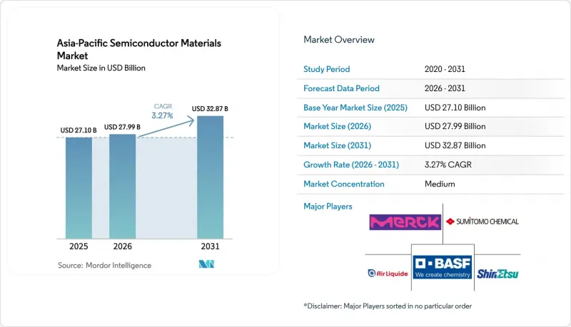
Mordor Intelligence에 의하면, 아시아태평양의 반도체 재료 시장 규모는 2025년 271억 달러로 평가되었고, 2026년에는 279억 9,000만 달러로 추정되고, 2026-2031년 CAGR 3.27%로 성장을 지속할 전망이며, 2031년에는 328억 7,000만 달러에 이를 것으로 예측됩니다.
본 보고서는 재료별(실리콘 웨이퍼, 실리콘 카바이드, 갈륨 비소, 기타), 용도별(제조(공정용 화학약품, 포토마스크), 기타), 패키징별(기판, 리드 프레임, 기타), 최종 사용자 산업별(가전, 통신 및 5G 인프라, 기타), 지역별로 분류되어 있습니다. 시장 예측은 금액(달러) 기준으로 제시되어 있습니다.
아시아태평양의 반도체 재료 시장 동향 및 인사이트
정부 주도의 ‘반도체 주권 기금’을 통한 중국, 일본, 한국의 신재료 팹 건설 가속화
동북아시아의 일부 정부는 전용 반도체 펀드를 활용하여 현지 재료 공장에 보조금을 지급함으로써 인증 주기를 단축하는 한편, 최첨단 팹에서 지역산 제품의 채택률을 높이고 있습니다. 한국에서는 경기도에 4,710억 달러 규모의 클러스터가 구축되어 있으며, 2030년까지 핵심 화학물질의 자급률 50%를 목표로 하고 있습니다. 일본은 TSMC의 구마모토 공장 확장 계획을 국내 포토레지스트 및 웨이퍼 공급업체와의 공동 연구개발 프로그램과 연계하고 있는 반면, 중국은 국산 CMP 슬러리, 전자 가스, 불소계 화학제품에 대한 자본 투자를 추진하고 있습니다. 이러한 협력적인 투자는 경기 순환에 따른 침체기에도 안정적인 수요를 뒷받침하며, 아시아태평양 반도체 재료 시장에 구조적인 성장 기반을 마련해 주고 있습니다.
중국과 일본에서 전기차 파워트레인용 SiC 및 GaN 채택 급증
전기차 제조업체들은 전도 손실을 줄이고 주행 거리를 연장하기 위해 실리콘 MOSFET에서 SiC 및 GaN 파워 디바이스로의 전환을 추진하고 있습니다. 중국의 수직 통합형 기판 제조업체 선구자들은 자동차 등급의 결함 밀도 기준을 충족하는 200mm SiC 웨이퍼 공급을 시작했으며, 이를 통해 현지 OEM 각사가 장기 계약을 체결할 수 있도록 지원하고 있습니다. 일본의 각 재료 제조업체들은 차량용 충전기를 위해 GaN-on-Si 에피택시에서 결정 품질 향상을 병행하여 추진하고 있습니다. 이러한 전환에 따라 재료 수요는 와이드 밴드갭 기판, 에피택시용 가스, 고온용 봉지재로 이동하고 있으며, 아시아태평양의 반도체 재료 시장은 실리콘을 핵심으로 하는 기존 틀을 넘어 확장되고 있습니다.
실리콘 및 희귀 금속 가격 변동이 팹의 이익률을 압박
현물 시장의 실리콘 웨이퍼와 도가니용 석영은 극소수의 광산에 집중된 공급망의 긴축을 배경으로 두 자릿수의 가격 변동을 보이고 있습니다. 수출 허가 규제의 영향으로 갈륨과 게르마늄 가격도 동시에 급등하고 있어, 각 팹 기업들은 장기 계약 재협상 및 상품 가격 변동 위험 헤지를 강요받고 있습니다. 재료비는 웨이퍼 제조 현금 원가의 25-30%를 차지하는 경우가 있어, 이러한 가격 변동은 수익성을 압박하고 확장 계획을 억제하게 되며, 아시아태평양 반도체 재료 시장은 설비 투자에 있어 신중한 자세를 유지하고 있습니다.
부문별 분석
2025년, 아시아태평양 반도체 재료 시장에서 실리콘 웨이퍼는 5nm 및 3nm 노드의 생산 능력 확대에 힘입어 37.74%라는 최대 점유율을 유지했습니다. 그러나 자동차의 전동화와 재생에너지 네트워크가 고전압 효율을 요구하는 가운데, 실리콘 카바이드(SiC)가 9.08%의 연평균 성장률(CAGR)로 확대되며 뚜렷한 성장 동력이 되고 있습니다. 이러한 변화로 인해 엄격한 표면 결함 기준을 충족하는 와이드 밴드갭 기판, 가스, 연마 슬러리 시장 규모가 확대되고 있습니다. GaN 및 GaAs 재료도 5G 기지국 및 RF 프런트최종 용도로 채택이 진행되고 있지만, 기판 비용이 양산 도입의 장벽이 되고 있습니다.
공정 혁신을 통해 200mm SiC 웨이퍼가 파일럿 규모로 생산되기 시작했고, 결함 밀도가 0.1cm-2 미만으로 낮아짐에 따라 자동차 부문에서 새로운 벤치마크가 확립되고 있습니다. 동시에, 한국화학기술연구원의 하이드로플루오로에테르 합성 분야의 획기적인 성과로 인해, 첨단 에칭용 화학물질의 현지 공급 안정성이 향상되고 있습니다. 이러한 기술적 이정표를 통해 단위 비용이 절감되고 신뢰성이 향상됨에 따라, ‘가격보다 성능’이라는 패러다임이 강화되어 아시아태평양 반도체 재료 시장의 조달 판단 방식이 재편되고 있습니다.
기타 혜택
- 엑셀 형식 시장 예측(ME) 시트
- 3개월간 애널리스트 지원
자주 묻는 질문
목차
제1장 서론
제2장 조사 방법
제3장 개요
제4장 시장 구도
제5장 시장 규모 및 성장 예측
제6장 경쟁 구도
제7장 시장 기회 및 향후 전망
AJY 26.09.01According to Mordor Intelligence, the Asia-Pacific semiconductor materials market size is expected to grow from USD 27.10 billion in 2025 to USD 27.99 billion in 2026 and is forecast to reach USD 32.87 billion by 2031 at 3.27% CAGR over 2026-2031.
This report is Segmented by Material (Silicon Wafers, Silicon Carbide, Gallium Arsenide, and More), Application (Fabrication [Process Chemicals, Photomasks], and More), Packaging (Substrates, Lead Frames, and More), End-User Industry (Consumer Electronics, Telecommunication and 5G Infrastructure, and More), and Geography. The Market Forecasts are Provided in Terms of Value (USD).
Asia-Pacific Semiconductor Materials Market Trends and Insights
Government-backed Chip Sovereignty Funds Accelerating New Material Fabs in China, Japan and Korea
Several Northeast-Asian governments are using dedicated chip funds to subsidize local material plants, shortening qualification cycles and lifting regional content in leading-edge fabs. In Korea, a USD 471 billion cluster in Gyeonggi Province targets 50% self-sufficiency in critical chemistries by 2030. Japan is tying TSMC's Kumamoto expansion to joint R&D programs with domestic photoresist and wafer suppliers, while China is channeling capital toward indigenous CMP slurries, electronic gases and fluorochemicals. These coordinated investments underpin steady demand even during cyclical downturns, giving the Asia-Pacific semiconductor materials market a structural growth floor.
Surge in SiC and GaN Adoption for EV Powertrains Across China and Japan
Electric-vehicle makers are shifting from silicon MOSFETs to SiC and GaN power devices to cut conduction losses and boost driving range. Chinese vertically integrated substrate pioneers have begun supplying 200 mm SiC wafers that meet automotive-grade defect density thresholds, helping local OEMs lock-in long-term contracts. Japanese material houses are parallel-tracking crystalline-quality improvements for GaN-on-Si epitaxy to serve on-board chargers. This transition is tilting material demand toward wide-bandgap substrates, epitaxial gases and high-temperature encapsulants, broadening the Asia-Pacific semiconductor materials market beyond its silicon core.
Volatile Silicon and Rare-Metal Prices Squeezing Fab Margins
Spot silicon-wafers and crucible-grade quartz have exhibited double-digit price swings amid tight supply chains concentrated in a handful of mines. Parallel spikes in gallium and germanium prices, following export-license restrictions, are forcing fabs to re-negotiate long-term contracts and hedge commodity exposure. Because material outlays can represent 25-30% of wafer-fabrication cash costs, these fluctuations compress profitability and temper expansion plans, keeping the Asia-Pacific semiconductor materials market on a cautious capital-expenditure footing.
Other drivers and restraints analyzed in the detailed report include:
- Mini/Micro-LED Ramp-up Driving Demand for High-Purity Metal-Organics in Korea and Taiwan
- ASEAN Re-shoring Initiatives Creating Green-field Chemical Plants for Backend Materials
- US/EU Export Controls Delaying Material Qualification in Mainland China
For complete list of drivers and restraints, kindly check the Table Of Contents.
Segment Analysis
Silicon Wafers retained the largest 37.74% share of the Asia-Pacific semiconductor materials market in 2025, supported by capacity additions at 5 nm and 3 nm nodes. Yet Silicon Carbide is the clear growth engine, expanding at 9.08% CAGR as vehicle electrification and renewable grids demand high-voltage efficiency. This shift is enlarging the Asia-Pacific semiconductor materials market size for wide-bandgap substrates, gases and polishing slurries that meet stringent surface-defect criteria. GaN and GaAs materials are also gaining traction for 5G base-stations and RF front-ends, even though substrate costs remain a cap on volume adoption.
Process innovation is bringing 200 mm SiC wafers to pilot scale, with defect densities below 0.1 cm-2 setting new automotive benchmarks. At the same time, the Korea Research Institute of Chemical Technology's breakthrough in hydrofluoroether synthesis improves local supply security for advanced etch chemistries. As these technical milestones reduce unit costs and raise reliability, they reinforce a performance-over-price paradigm that re-shapes procurement decisions within the Asia-Pacific semiconductor materials market.
Complete Report Scope:
- By Material
- Silicon Wafers
- Silicon Carbide (SiC)
- Gallium Arsenide (GaAs)
- Gallium Nitride (GaN)
- Silicon Germanium (SiGe)
- Indium Phosphide (InP)
- Copper Indium Gallium Selenide (CIGS)
- Molybdenum Disulfide (MoS?)
- Bismuth Telluride (Bi?Te?)
- Other Materials
- By Application
- Fabrication
- Process Chemicals
- Photomasks
- Electronic Gases
- Photoresist Ancillaries
- Sputtering Targets
- Silicon Wafers
- CMP Slurries and Pads
- Other Fabrication Materials
- Packaging
- Substrates
- Lead Frames
- Ceramic Packages
- Bonding Wire
- Encapsulation Resins
- Die-Attach Materials
- Other Packaging Materials
- Fabrication
- By End-user Industry
- Consumer Electronics
- Telecommunication and 5G Infrastructure
- Industrial and Manufacturing Automation
- Automotive and Mobility (EV, ADAS)
- Energy and Utility (Solar, Power Conversion)
- Data Centers and HPC
- Healthcare Devices
- Others
- By Geography
- Taiwan
- South Korea
- China
- Japan
- Rest of Asia-Pacific
List of Companies Covered in this Report:
- Shin-Etsu Chemical Co., Ltd.
- Showa Denko Materials Co., Ltd.
- Sumitomo Chemical Co., Ltd.
- Merck KGaA (incl. Versum Materials)
- Air Liquide S.A.
- BASF SE
- LG Chem Ltd.
- Indium Corporation
- Kyocera Corporation
- Henkel AG and Co. KGaA
- Dow Inc.
- JSR Corporation
- TOK (Tokyo Ohka Kogyo)
- DuPont de Nemours, Inc.
- Entegris, Inc.
- Linde plc
- SK Materials Co., Ltd.
- Toppan Photomask Co., Ltd.
- UTAC Holdings Ltd.
- Resonac
- Fujmi Corporation
- Mitsubishi Chemical Group Corp.
- Air Products and Chemicals, Inc.
Additional Benefits:
- The market estimate (ME) sheet in Excel format
- 3 months of analyst support
TABLE OF CONTENTS
1 INTRODUCTION
- 1.1 Study Assumptions and Market Definition
- 1.2 Scope of the Study
2 RESEARCH METHODOLOGY
3 EXECUTIVE SUMMARY
4 MARKET LANDSCAPE
- 4.1 Market Overview
- 4.2 Market Drivers
- 4.2.1 Government-backed Chip Sovereignty Funds Accelerating New Material Fabs in China, Japan and Korea
- 4.2.2 Surge in SiC and GaN Adoption for EV Powertrains Across China and Japan
- 4.2.3 Mini/Micro-LED Ramp-up Driving Demand for High-Purity Metal-Organics in Korea and Taiwan
- 4.2.4 ASEAN Re-shoring Initiatives Creating Green-field Chemical Plants for Backend Materials
- 4.2.5 Low-GWP Fluorinated Gas Mandates Boosting Replacement Chemistries
- 4.2.6 Heterogeneous Integration (2.5D/3D IC) Needs Novel Under-fill and Substrate Materials
- 4.3 Market Restraints
- 4.3.1 Volatile Silicon and Rare-Metal Prices Squeezing Fab Margins
- 4.3.2 US/EU Export Controls Delaying Material Qualification in Mainland China
- 4.3.3 Ultrapure-Water Scarcity in Taiwan and Singapore Hindering capacity Adds
- 4.3.4 Lengthy EHS Permitting for Chemical Plants in Korea
- 4.4 Industry Ecosystem Analysis
- 4.5 Technological Outlook
- 4.5.1 Heterogeneous Integration and Back-side Power Delivery
- 4.6 Porter's Five Forces Analysis
- 4.6.1 Bargaining Power of Suppliers
- 4.6.2 Bargaining Power of Buyers
- 4.6.3 Threat of New Entrants
- 4.6.4 Threat of Substitutes
- 4.6.5 Competitive Rivalry
5 MARKET SIZE AND GROWTH FORECASTS (VALUES)
- 5.1 By Material
- 5.1.1 Silicon Wafers
- 5.1.2 Silicon Carbide (SiC)
- 5.1.3 Gallium Arsenide (GaAs)
- 5.1.4 Gallium Nitride (GaN)
- 5.1.5 Silicon Germanium (SiGe)
- 5.1.6 Indium Phosphide (InP)
- 5.1.7 Copper Indium Gallium Selenide (CIGS)
- 5.1.8 Molybdenum Disulfide (MoS?)
- 5.1.9 Bismuth Telluride (Bi?Te?)
- 5.1.10 Other Materials
- 5.2 By Application
- 5.2.1 Fabrication
- 5.2.1.1 Process Chemicals
- 5.2.1.2 Photomasks
- 5.2.1.3 Electronic Gases
- 5.2.1.4 Photoresist Ancillaries
- 5.2.1.5 Sputtering Targets
- 5.2.1.6 Silicon Wafers
- 5.2.1.7 CMP Slurries and Pads
- 5.2.1.8 Other Fabrication Materials
- 5.2.2 Packaging
- 5.2.2.1 Substrates
- 5.2.2.2 Lead Frames
- 5.2.2.3 Ceramic Packages
- 5.2.2.4 Bonding Wire
- 5.2.2.5 Encapsulation Resins
- 5.2.2.6 Die-Attach Materials
- 5.2.2.7 Other Packaging Materials
- 5.2.1 Fabrication
- 5.3 By End-user Industry
- 5.3.1 Consumer Electronics
- 5.3.2 Telecommunication and 5G Infrastructure
- 5.3.3 Industrial and Manufacturing Automation
- 5.3.4 Automotive and Mobility (EV, ADAS)
- 5.3.5 Energy and Utility (Solar, Power Conversion)
- 5.3.6 Data Centers and HPC
- 5.3.7 Healthcare Devices
- 5.3.8 Others
- 5.4 By Geography
- 5.4.1 Taiwan
- 5.4.2 South Korea
- 5.4.3 China
- 5.4.4 Japan
- 5.4.5 Rest of Asia-Pacific
6 COMPETITIVE LANDSCAPE
- 6.1 Market Concentration
- 6.2 Strategic Moves (M&A, JVs, capacity Expansions)
- 6.3 Market Share Analysis
- 6.4 Company Profiles (includes Global Overview, Market Level Overview, Core Segments, Financials, Strategic Information, Market Rank/Share, Products and Services, Recent Developments)
- 6.4.1 Shin-Etsu Chemical Co., Ltd.
- 6.4.2 Showa Denko Materials Co., Ltd.
- 6.4.3 Sumitomo Chemical Co., Ltd.
- 6.4.4 Merck KGaA (incl. Versum Materials)
- 6.4.5 Air Liquide S.A.
- 6.4.6 BASF SE
- 6.4.7 LG Chem Ltd.
- 6.4.8 Indium Corporation
- 6.4.9 Kyocera Corporation
- 6.4.10 Henkel AG and Co. KGaA
- 6.4.11 Dow Inc.
- 6.4.12 JSR Corporation
- 6.4.13 TOK (Tokyo Ohka Kogyo)
- 6.4.14 DuPont de Nemours, Inc.
- 6.4.15 Entegris, Inc.
- 6.4.16 Linde plc
- 6.4.17 SK Materials Co., Ltd.
- 6.4.18 Toppan Photomask Co., Ltd.
- 6.4.19 UTAC Holdings Ltd.
- 6.4.20 Resonac
- 6.4.21 Fujmi Corporation
- 6.4.22 Mitsubishi Chemical Group Corp.
- 6.4.23 Air Products and Chemicals, Inc.
7 MARKET OPPORTUNITIES AND FUTURE OUTLOOK
- 7.1 White-space and Unmet-Need Assessment


