

|
시장보고서
상품코드
2119077
합성 단결정 다이아몬드 : 시장 점유율 분석, 업계 동향 및 통계, 성장 예측(2026-2031년)Synthetic Single Crystal Diamond - Market Share Analysis, Industry Trends & Statistics, Growth Forecasts (2026 - 2031) |
||||||
 Mordor Intelligence
Mordor Intelligence에 의하면, 합성 단결정 다이아몬드 시장 규모는 2025년에 19억 3,000만 달러로 평가되었습니다. 2026년 20억 9,000만 달러에서 2031년까지 30억 4,000만 달러로 확대되어 예측 기간(2026-2031년) CAGR은 7.78%가 된다고 전망되고 있습니다.
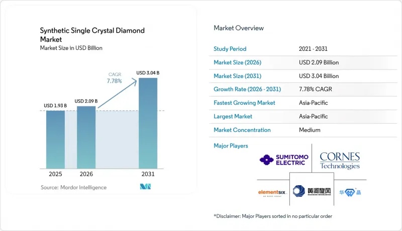
본 보고서는 제품 유형(단결정 다이아몬드 웨이퍼 등), 순도 등급(고순도 등), 제조 기술(화학기상증착법(CVD) 등), 용도(광전자 등), 최종 사용자 산업(자동차 등) 및 지역(아시아태평양, 북미 등)별로 분류되어 있습니다. 시장 전망은 금액(달러) 기준으로 제시되어 있습니다.
세계의 합성 단결정 다이아몬드 시장 동향 및 인사이트
전자 및 반도체 분야의 첨단 열 관리 솔루션에 대한 수요 증가
합성 단결정 다이아몬드 시장은 고출력 전자 플랫폼에서 기존 냉각 재료의 한계를 보완함으로써 혜택을 보고 있습니다. CVD 단결정 다이아몬드 열 확산기는 2,000-2,200 W/(m·K)의 열전도율을 실현할 수 있습니다. Element Six가 보고한 조사에 따르면, 열전도율은 2,200 W/(m·K)를 초과하며, 인용된 비교 기준에서 구리의 5배 이상에 달할 전망입니다. 따라서 다이아몬드는 고대역폭 메모리와 로직 다이를 결합한 패키지에서 열 전달의 제약을 완화할 수 있습니다. 이를 통해 이 소재는 수동적인 히트 스프레더에서 장치의 고성능화를 뒷받침하는 패키지 구성 요소로 그 역할을 전환하고 있습니다.
이러한 가능성은 GaN, 실리콘, SiC 각 플랫폼에까지 미치며, 각각의 기판에 맞추어 열 인터페이스가 설계되어 있습니다. 접합부 근처에 다이아몬드를 통합하면 적층형 소자 설계에서 열 저항을 저감할 수 있습니다. 패키징 아키텍처에서 더 많은 능동 소자가 근접하게 배치됨에 따라 이 기능의 중요성은 더욱 커지고 있습니다. 합성 단결정 다이아몬드 시장에서 이러한 설계가 보다 광범위한 생산 단계로 전환되기 위해서는 신뢰성 높은 접합, 일관된 표면 품질, 그리고 소자 가공과의 호환성이 필수적입니다. 또한, 자동차 및 통신용 파워 모듈에 대한 공식적인 열 인터페이스 요구 사항 역시, 보다 광범위한 채택에 앞서 추가적인 인증 절차를 필요로 합니다.
고품질·대면적 단결정 다이아몬드 기판용 CVD 기술 채택 확대
합성 단결정 다이아몬드 시장은 CVD 생산 능력에 대한 진입 장벽이 낮아진 것의 영향도 받고 있습니다. 실험실에서 배양된 보석용 다이아몬드의 성장으로 인해 마이크로파 플라즈마 CVD 장비의 비용이 낮아졌고, 반응기에 대한 전문 지식 기반이 확대되었습니다. 『Chemical &Engineering News』지의 보도에 따르면, 제조업체는 주얼리 등급용 반응로를 개조하여 반도체 등급 다이아몬드 성장에 활용할 수 있습니다. 이러한 발전으로 초기 설비 도입 장벽은 낮아졌지만, 전자 등급 생산에는 여전히 엄격한 공정 제어가 요구됩니다. 상업적인 주요 과제는 제조업체가 설비 비용 절감을 안정적인 대면적 기판 제조로 연결할 수 있느냐에 있습니다.
Element Six사와 Orbray사는 2026년 6월, 3인치 단결정 다이아몬드 기판용 재현성 있는 공정을 발표했습니다. 두 회사는 또한 4인치 기판 개발이 진행 중이며, Element Six사의 그레셤 공장에서 열접합용 2인치 웨이퍼가 양산 단계에 가까워지고 있음을 밝혔습니다. 기판이 커짐에 따라 1회 가동당 디바이스 처리 매수가 증가하며, 다이아몬드를 100mm 반도체 제조 장비와 호환시킬 수 있게 됩니다. 이러한 호환성 덕분에 이미 표준 리소그래피 및 박막 형성 장비를 사용하고 있는 고객의 경우 공정 중단을 최소화할 수 있습니다. 따라서 합성 단결정 다이아몬드 시장에서 웨이퍼 직경, 수율 및 표면 균일성은 주요 경쟁 요소가 됩니다.
HPHT 및 CVD 제조 시설에 필요한 막대한 설비 투자
전자 등급 CVD 생산에는 리액터 어레이, 진공 공정 시스템, 연마 장비, 계측 기기가 필요하며, 이 모든 것은 시설이 수익을 창출하기 전에 막대한 설비 투자가 필요합니다. 허난 황하 월윈드 사는 50대의 마이크로파 플라즈마 화학적 기상 증착(MPCVD) 장비를 사용하여 연간 2만 장의 히트 스프레더 웨이퍼를 생산하는 프로젝트의 1단계에 3억 6,000만 위안(5,000만 달러)을 투자했습니다. 이 프로젝트는 대면적 생산에 수반되는 설비 집약성을 여실히 보여줍니다. 또한, 전자 등급의 성장에는 더 긴 생산 주기와 엄격하게 제어된 플라즈마 조건이 필요하기 때문에 에너지 소비량도 높아집니다.
이러한 비용 요건으로 인해 기존 공급업체들은 소규모 신규 진출기업들에 비해 유리한 입지에 있습니다. Element Six, IIa Technologies 및 Applied Diamond는 자본 투자를 뒷받침할 수 있는 기존 기술력과 고객 관계를 보유하고 있습니다. 전력 인프라가 제한적이라는 점은 에너지 집약적 생산 지역에서의 그린필드 개발을 더욱 제약할 가능성이 있습니다. 그 결과, 합성 단결정 다이아몬드 시장에서는 생산 능력이 집중된 상태가 지속되는 한, 전자 등급 소재에 대한 프리미엄 가격 책정이 유지될 가능성이 있습니다. 수출 규제는 규정 준수 비용을 증가시키고, 첨단 합성 다이아몬드 소재의 최종 용도 선택지를 제한할 가능성이 있습니다.
부문별 분석
2025년, 단결정 다이아몬드 웨이퍼는 제품 유형별 매출의 42.53%를 차지했으며, 2031년까지 연평균 성장률(CAGR) 8.09%를 나타낼 것으로 예측됩니다. 이러한 위상은 반도체 기판, 광학 창, 히트 스프레더용 블랭크로서의 용도를 반영한 것입니다. 단결정 다이아몬드 웨이퍼 시장은 웨이퍼 크기의 확대에 따른 혜택을 받고 있는데, 이는 대형 포맷일수록 한 번의 생산 공정에서 더 많은 다이를 제조할 수 있기 때문입니다. 2026년에 발표된 3인치 공정 및 진행 중인 4인치 개발은 기존 반도체 제조 장비와 호환됩니다. 합성 단결정 다이아몬드 시장에서 웨이퍼는 치수 및 표면 품질의 엄격한 관리가 요구되는 고부가가치 전자·열 관련 용도에도 대응하고 있습니다.
단결정 다이아몬드 플레이트는 큰 횡방향 면적보다 두께 제어가 중요한 용도에 사용됩니다. 레이저, 레이더 및 광전자공학 사용자들은 열 확산 및 광학 기능을 위해 계속해서 이러한 형태를 필요로 하고 있습니다. 단결정 다이아몬드 필름은 가장 얇고 유연성이 가장 높은 제품 형태입니다. 그 중요성은 다이아몬드 상의 질화갈륨(GaN)을 이용한 고주파(RF) 전력 증폭기에서 커지고 있으며, 직접 성장 방식을 통해 열 계면 손실을 줄일 수 있습니다. 박막은 여전히 매출 규모가 가장 작은 부문이지만, 집적 냉각에의 응용을 통해 개별 히트 스프레더를 넘어서는 새로운 길이 열리고 있습니다. 합성 단결정 다이아몬드 업계는 모든 형태에서 품질을 유지하면서, 고객별 고유한 요구 사항에 맞추어 생산을 조정해 나가야 합니다.
고순도 다이아몬드는 2025년에 매출의 62.38%를 차지했으며, 2031년까지 연평균 성장률(CAGR) 8.45%로 성장할 것으로 전망됩니다. 전자, 양자 센싱 및 첨단 광학 응용 분야에서는 질소 농도가 극히 낮은 소재가 요구됩니다. 동위원소 농축된 탄소-12 다이아몬드는 양자 소자에서 스핀 코히어런스의 장기화에도 기여합니다. 2025년 연구에 따르면, 질소 농도가 0.8 ppm인 저질소 화학 기상 증착(CVD) 다이아몬드는 펄스 자기 측정에서 광자 샷 노이즈에 의해 제한되는 직류(DC) 자기장 감도를 달성한 것으로 밝혀졌습니다. 이러한 성능 요건이 합성 단결정 다이아몬드 시장에서 고순도 제품에 대한 프리미엄 가격을 뒷받침하고 있습니다.
표준 순도의 소재는 광학적 투명성이나 양자 코히어런스보다 1캐럿당 비용이 더 중요하게 여겨지는 절삭 공구 및 연마 용도에서 계속해서 사용되고 있습니다. 공급량이 증가하면 대량 생산 업체들이 표준 등급의 가격에 압박을 가할 가능성이 있습니다. 고순도 공급업체들은 공정 관리, 신뢰할 수 있는 사양, 그리고 최종 사용자와의 인증을 통해 경쟁하고 있습니다. 미국 및 유럽의 국방 관련 양자 센싱 프로그램에서 수요는 엄격하게 관리되는 소재에 대한 또 다른 수요원이 되고 있습니다. 합성 단결정 다이아몬드 업계는 대량 생산되는 산업용 등급과 용도 인증을 받은 프리미엄 등급 사이에서 점점 더 양극화되고 있습니다.
지역별 분석
아시아태평양은 2025년 합성 단결정 다이아몬드 시장 점유율의 55.62%를 차지했으며, 2031년까지 연평균 성장률(CAGR) 8.41%로 성장할 것으로 전망됩니다. 중국의 산업용 다이아몬드 기반은 연마재 생산에서 전자 등급 히트 스프레더 및 CVD 기판으로 전환되고 있습니다. 허난 황하 월윈드 사는 2026년 자회사인 허난 펑창(河南風創)을 통해 8인치 다이아몬드 히트 스프레더 생산 라인을 개발했습니다. 1단계에서는 3억 6,000만 위안(5,000만 달러)을 투자하여 50대의 MPCVD 장비를 도입하고, 칩 패키징 용도로 화웨이 및 SMIC의 검증을 거친 제품을 생산했습니다. 이를 통해 해당 지역은 대량 생산 능력과 확대되는 기술 기반 고객층을 모두 확보했습니다.
일본은 정밀하고 전문성이 높은 제품에 초점을 맞추어 중국의 규모를 보완하고 있습니다. Orbray사와 Element Six사는 재현성 있는 3인치 단결정 다이아몬드 공정을 확립했습니다. EDP사는 1인치 반도체 웨이퍼를 시장에 출시하고, 2인치 포맷용 모자이크 결정 기술을 개발했습니다. 한국은 다이아몬드 기판을 평가하고 있는 반도체 장비 제조업체를 통해 중요한 역할을 수행하고 있습니다. 인도에서는 합성 다이아몬드에 관한 세관 신고 요건이 2024년 12월에 발효되어 무역 분류 제도가 공식적으로 확립되었습니다. 이러한 동향은 투자 계획 및 국경을 초월한 공급에 있어 사업 환경의 개선으로 이어지고 있습니다.
북미 및 유럽은 생산량보다는 기술적 리더십, 국방 수요, 그리고 용도 인증을 통해 특징지어집니다. ARPA-E의 LADDIS 및 UWBGS 프로그램은 국방 및 반도체 용도를 위한 100mm 이상의 단결정 웨이퍼와 관련된 Element Six의 노력을 지원했습니다. Diamond Foundry는 2025년 스페인 토르히요에 상업용 CVD 시설을 개설했습니다. Diamfab사는 2026년 그르노블에 반도체 등급 합성 다이아몬드용 파일럿 플랜트를 개설했습니다. 이 지역들의 합성 단결정 다이아몬드 시장은 기술 인증 절차와 국내 공급망 구축의 혜택을 받고 있습니다. 남미, 중동 및 아프리카는 여전히 초기 단계 시장이며, 수요는 산업용 절단, 광업, 석유 및 가스용 공구에 집중되어 있습니다. 이 지역에서는 예측 기간 동안 전자 등급에 대한 수요는 제한적이지만, 양산 등급 공급업체에게는 수출 다각화의 기회가 될 것입니다.
기타 혜택 :
- 엑셀 형식 시장 예측(ME) 시트
- 3개월간의 애널리스트 지원
자주 묻는 질문
목차
제1장 서론
제2장 조사 방법
제3장 개요
제4장 시장 구도
제5장 시장 규모 및 성장 예측
제6장 경쟁 구도
제7장 시장 기회 및 향후 전망
KTH 26.09.02According to Mordor Intelligence, the synthetic single crystal diamond market size was estimated at USD 1.93 billion in 2025 and is estimated to grow from USD 2.09 billion in 2026 to USD 3.04 billion by 2031, at a CAGR of 7.78% during the forecast period (2026-2031).
This report is Segmented by Product Type (Single Crystal Diamond Wafers and More), Purity Grade (High Purity and More), Manufacturing Technology (Chemical Vapor Deposition (CVD) and More), Application (Optoelectronics and More), End-User Industry (Automotive and More), and Geography (Asia-Pacific, North America, and More). The Market Forecasts are Provided in Terms of Value (USD).
Global Synthetic Single Crystal Diamond Market Trends and Insights
Growing Demand for Advanced Thermal Management Solutions in Electronics and Semiconductors
The synthetic single crystal diamond market benefits from the limitations of conventional cooling materials in high-power electronic platforms. CVD single-crystal diamond heat spreaders can deliver thermal conductivities of 2,000-2,200 W/(m*K). Research reported by Element Six showed thermal conductivity above 2,200 W/(m*K), more than five times that of copper in the cited comparison. Diamond can therefore reduce heat transfer constraints in packages that combine high-bandwidth memory and logic dies. This shifts the material from a passive heat spreader toward a package component that supports higher device performance.
The opportunity extends across GaN, silicon, and SiC platforms where thermal interfaces are engineered for the relevant substrate. Near-junction diamond integration can limit thermal resistance in stacked device designs. This capability is relevant as packaging architectures place more active components in close proximity. The synthetic single crystal diamond market depends on reliable bonding, consistent surface quality, and compatibility with device processing before these designs can move into wider production. Formal thermal interface requirements in automotive and telecommunications power modules also add a qualification step before broader adoption.
Increasing Adoption of CVD Technology for High-Quality, Large-Area Single Crystal Diamond Substrates
The synthetic single crystal diamond market is also shaped by lower barriers to CVD capacity. The growth of lab-grown jewelry diamonds reduced the cost of microwave plasma CVD equipment and expanded the base of reactor expertise. Chemical & Engineering News reported that producers can modify jewelry-grade reactors for semiconductor-grade diamond growth. This development lowers initial equipment barriers, although electronic-grade production still requires demanding process control. The main commercial question is whether producers can translate lower equipment costs into consistent large-area substrates.
Element Six and Orbray announced a reproducible process for 3-inch single crystal diamond substrates in June 2026. The companies also stated that 4-inch development was underway and that 2-inch wafers for thermal bonding were approaching volume production at Element Six's Gresham facility. Larger substrates allow more devices to be processed per run and align diamond with 100 mm semiconductor tool sets. This compatibility can reduce process disruption for customers who already use standard lithography and deposition equipment. For the synthetic single crystal diamond market, wafer diameter, yield, and surface uniformity are therefore central competitive factors.
High Capital Investment Requirements for HPHT and CVD Manufacturing Facilities
Electronic-grade CVD production requires reactor arrays, vacuum process systems, polishing equipment, and metrology tools, all of which demand significant capital investment before a facility can generate revenue. Henan Huanghe Whirlwind committed CNY 360 million (USD 50 million) to the first phase of a project that uses 50 Microwave Plasma Chemical Vapor Deposition (MPCVD) machines to produce 20,000 heat spreader wafers per year. This project illustrates the equipment intensity involved in large-area production. Energy consumption is also high, as electronic-grade growth requires longer production runs and closely controlled plasma conditions.
These cost requirements place established suppliers in a stronger position relative to smaller new entrants. Element Six, IIa Technologies, and Applied Diamond possess existing technical capabilities and customer relationships that support capital deployment. Limited power infrastructure can further restrict greenfield development in energy-intensive production regions. As a result, the synthetic single crystal diamond market may retain premium pricing for electronic-grade material while capacity remains concentrated. Export controls add compliance costs and can limit end-use options for advanced synthetic diamond materials.
Other drivers and restraints analyzed in the detailed report include:
- Rising Demand for High-Precision Cutting Tools and Abrasive Applications
- Expanding Development of Quantum Sensing and Diamond-Based Electronic Devices
- Lengthy Qualification Cycles and Yield Challenges in Semiconductor Applications
For complete list of drivers and restraints, kindly check the Table Of Contents.
Segment Analysis
Single Crystal Diamond Wafers held 42.53% of product-type revenue in 2025 and are forecast to grow at an 8.09% CAGR through 2031. This position reflects their use as semiconductor substrates, optical windows, and heat spreader blanks. The market for single crystal diamond wafers benefits from wafer-size scaling, as larger formats support more dies per production run. The 3-inch process announced in 2026, along with ongoing 4-inch development, is compatible with existing semiconductor equipment. Within the synthetic single crystal diamond market, wafers also support higher-value electronic and thermal applications that require controlled dimensions and surface quality.
Single Crystal Diamond Plates are used in applications where thickness control is more important than large lateral area. Laser, radar, and optoelectronic users continue to require these forms for thermal spreading and optical functions. Single Crystal Diamond Films are the thinnest and most flexible product form. Their relevance is growing in Gallium Nitride (GaN)-on-diamond radio frequency (RF) power amplifiers, where direct growth can reduce thermal interface losses. Films remain the smallest revenue segment, but their use in integrated cooling creates a path beyond discrete heat spreaders. The synthetic single crystal diamond industry must maintain quality across all form factors while adapting production to distinct customer requirements.
High-purity diamond held 62.38% of revenue in 2025 and is forecast to grow at an 8.45% CAGR through 2031. Electronics, quantum sensing, and advanced optical applications require materials with very low nitrogen concentration. Isotopically enriched carbon-12 diamond also supports longer spin coherence for quantum devices. A 2025 study found that a low-nitrogen chemical vapor deposition (CVD) diamond with 0.8 ppm nitrogen achieved photon-shot-noise-limited direct current (DC) magnetic field sensitivity in pulsed magnetometry. These performance requirements sustain the high-purity premium in the synthetic single crystal diamond market.
Standard purity material continues to serve cutting tools and abrasive applications, where cost per carat matters more than optical transparency or quantum coherence. High-volume producers can pressure standard-grade pricing when supply expands. High-purity suppliers compete through process control, reliable specifications, and qualifications with end users. Demand from defense-linked quantum sensing programs in the United States and Europe adds a further source of demand for highly controlled materials. The synthetic single crystal diamond industry is increasingly divided between high-volume industrial grades and application-qualified premium grades.
Complete Report Scope:
- By Product Type
- Single Crystal Diamond Wafers
- Single Crystal Diamond Plates
- Single Crystal Diamond Films
- By Purity Grade
- High Purity
- Standard Purity
- By Manufacturing Technology
- High Pressure High Temperature (HPHT)
- Chemical Vapor Deposition (CVD)
- By Application
- Electronics and Semiconductors
- Thermal Management
- Optoelectronics
- Cutting Tools
- Jewelry (Gemstones)
- Medical Devices
- Quantum Technologies
- Other Applications
- By End-User Industry
- Automotive
- Electronics and Semiconductor
- Industrial Manufacturing
- Healthcare
- Aerospace and Defense
- Consumer Goods
- Research and Academic Institutions
- Other End-Use Industries
- By Geography
- Asia-Pacific
- China
- India
- Japan
- South Korea
- Rest of Asia-Pacific
- North America
- United States
- Canada
- Mexico
- Europe
- Germany
- United Kingdom
- France
- Italy
- Russia
- Rest of Europe
- South America
- Brazil
- Argentina
- Rest of South America
- Middle-East and Africa
- Saudi Arabia
- South Africa
- Rest of Middle-East and Africa
- Asia-Pacific
Geography Analysis
Asia-Pacific held 55.62% of the synthetic single crystal diamond market share in 2025 and is forecast to grow at an 8.41% CAGR through 2031. China's industrial diamond base is shifting from abrasive production toward electronic-grade thermal spreaders and CVD substrates. Henan Huanghe Whirlwind developed an 8-inch diamond heat spreader production line through its Henan Fengchuang subsidiary in 2026. The first phase involved CNY 360 million (USD 50 million), 50 MPCVD units, and products verified by Huawei and SMIC for chip packaging applications. This gives the region both volume production capability and a growing technical customer base.
Japan complements China's scale with a focus on precise and specialized products. Orbray and Element Six established a reproducible 3-inch single crystal diamond process. EDP Co., Ltd. launched 1-inch semiconductor wafers and developed mosaic crystal technology for 2-inch formats. South Korea is relevant through semiconductor equipment companies evaluating diamond substrates. India's customs declaration requirements for synthetic diamonds took effect in December 2024, formalizing the trade classification system. These developments improve the operating environment for investment planning and cross-border supply.
North America and Europe are defined more by technology leadership, defense demand, and application qualifications than by manufacturing volume. ARPA-E's LADDIS and UWBGS programs supported Element Six's work on 100 mm or larger single crystal wafers for defense and semiconductor applications. Diamond Foundry opened a commercial CVD facility in Trujillo, Spain, in 2025. Diamfab opened a pilot plant in Grenoble in 2026 for semiconductor-grade synthetic diamond. The synthetic single crystal diamond market in these regions benefits from technical qualification pathways and domestic supply chain development. South America, the Middle-East, and Africa remain early-stage markets, with demand centered on industrial cutting, mining, and oil and gas tooling. These regions have limited electronic-grade demand during the forecast period, but offer export diversification opportunities for volume-grade suppliers.
- Advanced Diamond Technologies
- Applied Diamond Inc.
- Cornes Technologies Limited
- CR GEMS Superabrasives Co., Ltd.
- Diamond Materials GmbH
- Element Six UK Ltd.
- Henan Huanghe Whirlwind Co., Ltd.
- Henan Liliang Diamond Co., Ltd.
- IIa Technologies
- Mikrotek Machines Ltd.
- New Diamond Technology LLC
- Orbray Co., Ltd.
- SP3 Diamond Technologies, Inc.
- Sumitomo Electric Industries, Ltd.
- Zhengzhou Sino-Crystal Diamond Co., Ltd.
Additional Benefits:
- The market estimate (ME) sheet in Excel format
- 3 months of analyst support
TABLE OF CONTENTS
1 Introduction
- 1.1 Study Assumptions and Market Definition
- 1.2 Scope of the Study
2 Research Methodology
3 Executive Summary
4 Market Landscape
- 4.1 Market Overview
- 4.2 Market Drivers
- 4.2.1 Growing Demand for Advanced Thermal Management Solutions in Electronics and Semiconductors
- 4.2.2 Increasing Adoption of CVD Technology for High-Quality, Large-Area Single Crystal Diamond Substrates
- 4.2.3 Rising Demand for High-Precision Cutting Tools and Abrasive Applications
- 4.2.4 Expanding Development of Quantum Sensing and Diamond-Based Electronic Devices
- 4.2.5 Growth of AI Infrastructure and High-Power Computing Driving Advanced Cooling Requirements
- 4.3 Market Restraints
- 4.3.1 High Capital Investment Requirements for HPHT and CVD Manufacturing Facilities
- 4.3.2 Lengthy Qualification Cycles and Yield Challenges in Semiconductor Applications
- 4.3.3 Export Control Regulations and End-Use Restrictions for Advanced Synthetic Diamond Materials
- 4.4 Value Chain Analysis
- 4.5 Porter's Five Forces Analysis
- 4.5.1 Threat of New Entrants
- 4.5.2 Bargaining Power of Suppliers
- 4.5.3 Bargaining Power of Buyers
- 4.5.4 Threat of Substitutes
- 4.5.5 Competitive Rivalry
5 Market Size and Growth Forecasts (Value)
- 5.1 By Product Type
- 5.1.1 Single Crystal Diamond Wafers
- 5.1.2 Single Crystal Diamond Plates
- 5.1.3 Single Crystal Diamond Films
- 5.2 By Purity Grade
- 5.2.1 High Purity
- 5.2.2 Standard Purity
- 5.3 By Manufacturing Technology
- 5.3.1 High Pressure High Temperature (HPHT)
- 5.3.2 Chemical Vapor Deposition (CVD)
- 5.4 By Application
- 5.4.1 Electronics and Semiconductors
- 5.4.2 Thermal Management
- 5.4.3 Optoelectronics
- 5.4.4 Cutting Tools
- 5.4.5 Jewelry (Gemstones)
- 5.4.6 Medical Devices
- 5.4.7 Quantum Technologies
- 5.4.8 Other Applications
- 5.5 By End-User Industry
- 5.5.1 Automotive
- 5.5.2 Electronics and Semiconductor
- 5.5.3 Industrial Manufacturing
- 5.5.4 Healthcare
- 5.5.5 Aerospace and Defense
- 5.5.6 Consumer Goods
- 5.5.7 Research and Academic Institutions
- 5.5.8 Other End-Use Industries
- 5.6 By Geography
- 5.6.1 Asia-Pacific
- 5.6.1.1 China
- 5.6.1.2 India
- 5.6.1.3 Japan
- 5.6.1.4 South Korea
- 5.6.1.5 Rest of Asia-Pacific
- 5.6.2 North America
- 5.6.2.1 United States
- 5.6.2.2 Canada
- 5.6.2.3 Mexico
- 5.6.3 Europe
- 5.6.3.1 Germany
- 5.6.3.2 United Kingdom
- 5.6.3.3 France
- 5.6.3.4 Italy
- 5.6.3.5 Russia
- 5.6.3.6 Rest of Europe
- 5.6.4 South America
- 5.6.4.1 Brazil
- 5.6.4.2 Argentina
- 5.6.4.3 Rest of South America
- 5.6.5 Middle-East and Africa
- 5.6.5.1 Saudi Arabia
- 5.6.5.2 South Africa
- 5.6.5.3 Rest of Middle-East and Africa
- 5.6.1 Asia-Pacific
6 Competitive Landscape
- 6.1 Market Concentration
- 6.2 Strategic Moves
- 6.3 Market Share (%)/Ranking Analysis
- 6.4 Company Profiles (includes Global Overview, Market Overview, Core Segments, Financials as available, Strategic Information, Products and Services, and Recent Developments)
- 6.4.1 Advanced Diamond Technologies
- 6.4.2 Applied Diamond Inc.
- 6.4.3 Cornes Technologies Limited
- 6.4.4 CR GEMS Superabrasives Co., Ltd.
- 6.4.5 Diamond Materials GmbH
- 6.4.6 Element Six UK Ltd.
- 6.4.7 Henan Huanghe Whirlwind Co., Ltd.
- 6.4.8 Henan Liliang Diamond Co., Ltd.
- 6.4.9 IIa Technologies
- 6.4.10 Mikrotek Machines Ltd.
- 6.4.11 New Diamond Technology LLC
- 6.4.12 Orbray Co., Ltd.
- 6.4.13 SP3 Diamond Technologies, Inc.
- 6.4.14 Sumitomo Electric Industries, Ltd.
- 6.4.15 Zhengzhou Sino-Crystal Diamond Co., Ltd.
7 Market Opportunities and Future Outlook
- 7.1 White-Space and Unmet-Need Assessment


