

|
시장보고서
상품코드
2119387
반도체 첨단 패키징 재료 : 시장 점유율 분석, 업계 동향 및 통계, 성장 예측(2026-2031년)Semiconductor Advanced Packaging Materials - Market Share Analysis, Industry Trends & Statistics, Growth Forecasts (2026 - 2031) |
||||||
 Mordor Intelligence
Mordor Intelligence에 의하면, 반도체 첨단 패키징 재료 시장 규모는 2025년에 185억 6,000만 달러로 평가되었습니다. 예측 기간(2026-2031년) CAGR 9.06%로 확대되어 2026년 201억 1,000만 달러에서 2031년에는 310억 3,000만 달러에 이를 전망입니다.
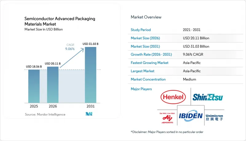
본 보고서는 재료 유형(기판 등), 패키징 기술(플립칩 패키징 등), 용도(로직 및 AI 프로세서 등), 지역(아시아태평양, 북미, 유럽, 남미, 중동 및 아프리카)별로 분류되어 있습니다. 시장 예측은 금액(달러) 기준으로 제시되어 있습니다.
세계의 반도체 첨단 패키징 재료 시장 동향 및 인사이트
AI 및 HBM 패키지의 복잡화, 소재 BOM 확대를 견인
HBM 세대가 진화함에 따라 AI 패키지에 필요한 재료량이 증가하고 있습니다. 2026년에 양산이 시작된 HBM4에서는 다이 간 물리적 인터페이스 부근에서 더 높은 열전도율을 가진 성형 언더필 배합이 요구되고 있습니다. SK하이닉스는 2026년 5월 26일, 실리콘 기반의 냉각 소자를 HBM 패키지에 통합한 ‘iHBM’ 열 솔루션을 발표했습니다. 이 회사에 따르면, 이 솔루션은 자사의 ‘Advanced Mass Reflow Molded Underfill(MR-MUF)’ 공정과의 호환성을 유지하면서 열저항을 30% 저감한다고 합니다. 삼성의 하이브리드 구리 본딩 방식과 SK하이닉스의 MR-MUF 접근 방식은 언더필 재료에 대해 서로 다른 인증 프로세스를 만들어내고 있습니다. 고객이 선택한 본딩 방식에 조기에 대응한 공급업체는 인증 상태를 확보할 수 있지만, 여러 방식에 대응하는 공급업체는 추가적인 개발 요건에 직면하게 됩니다.
이종 통합 및 치플렛 채택으로 인터페이스 층 증가
치플릿 아키텍처에서는 다이 간 및 다이와 인터포저 간의 인터페이스가 추가되며, 여기에는 언더필, 접착제 및 유전체 처리가 필요합니다. 이로 인해 단순히 단위 출하량이 증가할 뿐만 아니라, 패키지당 재료 요구량도 증가하게 됩니다. 인텔이 2025년에 출원한 특허에 따르면, 치플릿의 메탈라이제이션이 호스트 집적회로(IC)의 백엔드 오브 라인(BEOL) 층에 직접 본딩된다고 기술되어 있으며, 이로 인해 실리콘 인터포저의 역할은 축소되고 유기 재배선층(RDL) 유전체 재료의 역할은 확대될 가능성이 있습니다. 따라서 패키지 설계에서 인터페이스의 수나 재료의 유형가 증가하면, 반도체 첨단 패키징 재료 시장에 영향을 미치게 됩니다. 이종 집적 및 하이브리드 본딩은 칩렛 개발에서 여전히 핵심적인 기술 경로로 남아 있습니다. 파운드리에서 승인한 재료 목록은 전문적인 패키징 프로그램에 참여하기 위한 실질적인 요건이 될 수 있습니다.
높은 소재 인증 비용이 신소재 도입 속도를 제약
신소재 도입에는 대개 18-24개월의 고객 인증 주기가 필요합니다. 시험에서는 일반적으로 열 사이클, 습기 민감도, 기계적 신뢰성이 평가되며, 많은 경우 웨이퍼 레벨 공정 통합도 포함됩니다. 특정 패키징 노드에서 인증이 완료되었더라도, 패키지의 형상, 층 수 또는 본딩 아키텍처가 변경된 경우 해당 인증은 차세대 제품에는 적용되지 않을 수 있습니다. 이러한 요건으로 인해 반도체 첨단 패키징 재료 시장에서 기존 인증 공급업체의 입지가 강화되고 있습니다. 승인된 소재에 대한 장기 공급 계약 및 생산 능력 확보 역시 이러한 입지를 더욱 뒷받침하고 있습니다. 2.5D 및 3D 패키징 승인 공급업체 목록에 포함되지 않은 공급업체는 차세대 패키지가 등장하기 전에 시장에 진입할 기회가 제한될 수 있습니다.
부문별 분석
2025년, 기판은 첨단 반도체 패키징 재료 시장 점유율의 41.12%를 차지했습니다. 이러한 위상은 다양한 첨단 패키징 유형에서 기판이 수행하는 구조적 및 전기적 배선상의 역할을 반영한 것입니다. ABF(빌드업 필름), 구리 박판 적층 기판 및 솔더 레지스트가 기판 소재의 핵심을 구성합니다. 대형 AI 서버용 패키지의 경우, 단위당 기판 면적이 더 많이 필요한 반면, 층 수가 늘어남에 따라 빌드업 필름의 소비량도 증가합니다. IEEE 전자 패키징 학회에 따르면, 최첨단 재분배 층(RDL) 구현에는 현재 2µm의 선폭이 채택되고 있으며, 목표 유전율은 2.0 이하로 전환되고 있습니다. 패키지 신호에 대한 수요가 높아지는 가운데, 이러한 요구 사항은 저손실 유전체 재료의 사용을 촉진하고 있습니다.
다이 어태치 소재는 2026년부터 2031년까지 연평균 성장률(CAGR) 9.53%를 나타낼 것으로 예측되며, 이 소재 그룹 내에서 가장 높은 성장률을 보일 것으로 전망됩니다. 소결 은 다이 부착 필름은 기존의 폴리머 페이스트로는 열적 요구 사항 및 신뢰성 요구 사항을 충족할 수 없는 파워 일렉트로닉스 및 고밀도 플립 칩 용도에서 채택이 확대되고 있습니다. AI 및 고성능 컴퓨팅용 패키지에서 플립 칩 기술의 보급이 확대됨에 따라 언더필에 대한 수요도 증가하고 있습니다. 또한, 대형 플립 칩 BGA 구성에서도 갭 높이가 낮은 다이 연결에 대응할 수 있는 소재가 요구되고 있습니다. 봉지 재료는 모바일 기기 및 IoT 기기의 대량 생산을 뒷받침하고 있으며, 한편 열 인터페이스 재료, 솔더 재료, 빌드업 필름의 중요성도 점점 더 커지고 있습니다. 반도체 첨단 패키징 재료 업계는 방열, 기계적 신뢰성, 전기적 성능의 균형을 맞추기 위해 이 모든 범주에 의존하고 있습니다.
지역별 분석
아시아태평양은 2025년에 반도체 첨단 패키징 재료 시장 점유율의 39.18%를 차지했으며, 2031년까지 연평균 성장률(CAGR) 9.88%로 성장할 것으로 전망됩니다. 이 지역에는 첨단 패키징 생산 능력과 반도체 소재 생산이 집중되어 있습니다. 대만은 계속해서 IC 기판 생산의 주요 거점으로 자리 잡고 있습니다. 일본은 아지노모토 빌드업 필름(ABF), 봉지재 및 첨단 유전체 폴리머를 세계 공급망에 공급하고 있습니다. 한국은 AI 가속기 및 서버용 CPU 수요에 힘입어 패키징 기판 분야에서 활발한 활동을 이어가고 있습니다. 인도는 국내 조립 및 패키징 계획을 지원하는 소재 응용 거점이자 혁신 센터로 부상하고 있습니다.
북미는 AI 칩 설계 활동이 가장 집중된 지역이지만, 설계 수요에 비해 생산 자산은 여전히 제한적입니다. 이러한 격차로 인해 이 지역은 첨단 패키징 재료 수입에 계속 의존하고 있습니다. 유럽에서는 오스트리아의 AT&S사가 주도적인 역할을 하고 있으며, 이 회사는 2025년 6월 레오벤에 유럽 최초의 IC 기판 생산 시설을 개소했습니다. 이 프로젝트에는 5억 유로가 넘는 투자가 이루어졌으며, 소식통에 따르면 그 금액은 5억 5,000만 달러에 달하는 것으로 보도되고 있습니다. 독일에서는 헨켈(Henkel)사의 언더필, 봉지재, 열 관리 소재 제품 포트폴리오를 통해 소재 공급업체들의 활동이 활발히 이루어지고 있습니다. 이러한 역량을 바탕으로 유럽은 기판 제조 및 특수 소재 개발 분야에서 확고한 입지를 구축하고 있습니다.
2025년에도 남미, 중동 및 아프리카는 반도체 첨단 패키징 재료 시장에 대한 기여도가 여전히 낮은 수준을 유지했습니다. 멕시코에서는 전자제품 제조에 대한 투자가 유치되고 있으며, 특히 자동차 및 소비자 가전 조립 분야에서 봉지재와 접착제에 대한 현지 수요가 발생할 가능성이 있습니다. 중동 국가들은 국가 기술 프로그램을 통해 반도체 공급망 인프라에 투자하고 있지만, 해당 지역의 첨단 패키징 재료 생산 능력은 여전히 제한적입니다. 남아프리카공화국 및 기타 아프리카 국가들은 반도체 패키징보다는 하류 단계인 전자기기 조립에 중점을 두고 있습니다. 이들 국가의 향후 기여도는 2020년대 후반에 걸쳐 진행될 반도체 공급망의 광범위한 지역화에 달려 있습니다.
기타 혜택 :
- 엑셀 형식 시장 예측(ME) 시트
- 3개월간의 애널리스트 지원
자주 묻는 질문
목차
제1장 서론
제2장 조사 방법
제3장 개요
제4장 시장 구도
제5장 시장 규모 및 성장 예측
제6장 경쟁 구도
제7장 시장 기회 및 향후 전망
KTH 26.09.02According to Mordor Intelligence, the semiconductor advanced packaging materials market size is estimated at USD 18.56 billion in 2025 and is estimated to grow from USD 20.11 billion in 2026 to USD 31.03 billion by 2031, at a CAGR of 9.06% during the forecast period (2026-2031).
This report is Segmented by Material Type (Substrates and More), Packaging Technology (Flip-Chip Packaging and More), Application (Logic and AI Processors and More), and Geography (Asia-Pacific, North America, Europe, South America, and Middle-East and Africa). The Market Forecasts are Provided in Terms of Value (USD).
Global Semiconductor Advanced Packaging Materials Market Trends and Insights
AI and HBM Package Complexity Driving Materials Bill-of-Materials Expansion
Each HBM generation increases the material content required in an AI package. HBM4 entered production in 2026 and requires molded underfill formulations with higher thermal conductivity near the die-to-die physical interface. SK hynix introduced its iHBM thermal solution on May 26, 2026, integrating silicon-based cooling elements into the HBM package. The company stated that the solution reduces thermal resistance by 30% while maintaining compatibility with its Advanced Mass Reflow Molded Underfill (MR-MUF) process. Samsung's hybrid copper bonding route and SK hynix's MR-MUF approach create separate qualification paths for underfill materials. Suppliers that align early with a customer's selected bonding route can secure qualified status, while suppliers serving multiple routes face additional development requirements.
Heterogeneous Integration and Chiplet Adoption Multiplying Interface Layers
Chiplet architectures add die-to-die and die-to-interposer interfaces that require underfill, adhesive, and dielectric treatment. This increases the material requirement for each package rather than simply increasing unit shipments. Intel's 2025 patent filings described chiplet metallization directly bonded to host integrated circuit (IC) back-end-of-line layers, which could reduce the role of silicon interposers and increase the role of organic redistribution-layer dielectric materials. Therefore, the semiconductor advanced packaging materials market is affected when package designs use more interfaces and more material types. Heterogeneous integration and hybrid bonding remain central technology paths for chiplet development. Foundry-approved material lists can become a practical requirement for participation in specialized packaging programs.
High Material Qualification Costs Constraining New Material Adoption Velocity
New materials often require an 18- to 24-month customer qualification cycle. Testing typically covers thermal cycling, moisture sensitivity, mechanical reliability, and, in many cases, wafer-level process integration. A completed qualification for one packaging node may not apply to the next generation if package geometry, layer count, or bonding architecture changes. This requirement strengthens the position of existing approved suppliers in the semiconductor advanced packaging materials market. Long-term supply agreements and capacity reservations for approved materials further support this position. Suppliers outside approved vendor lists for 2.5D and 3D packaging may have limited opportunities to enter the market before the next package generation.
Other drivers and restraints analyzed in the detailed report include:
- ABF and Low-Loss Material Qualification Creating Structural Supply Constraints
- TIM1.5 and Package-Level Thermal Innovation Emerging as a Distinct Market Segment
- PFAS Substitution and Chemical Traceability: Introducing Multi-Year Compliance Costs
For complete list of drivers and restraints, kindly check the Table Of Contents.
Segment Analysis
Substrates accounted for 41.12% of the semiconductor advanced packaging materials market share in 2025. Their position reflected the structural and electrical routing role they play across advanced package types. ABF build-up film, copper-clad laminates, and solder resist form the core substrate material set. Larger AI server packages require more substrate area per unit, while higher layer counts increase build-up film consumption. The IEEE Electronics Packaging Society states that leading redistribution-layer implementations now use 2 µm linewidths, while target dielectric constants are moving toward 2.0 or below. These requirements support the use of low-loss dielectric materials as demand for package signals increases.
Die attach materials are expected to register a 9.53% CAGR from 2026 to 2031, the highest growth rate within this material grouping. Sintered silver die attach films are gaining use in power electronics and dense flip-chip applications, where conventional polymer pastes cannot meet thermal and reliability requirements. Underfill demand is rising with the deeper adoption of flip-chip technology in AI and high-performance computing packages. Large-body flip-chip BGA configurations also require materials that can manage low-gap-height die connections. Encapsulation materials support high-volume mobile and IoT assembly, while thermal interface materials, solder materials, and build-up films are becoming more important. The semiconductor advanced packaging materials industry relies on all these categories to balance heat removal, mechanical reliability, and electrical performance.
Complete Report Scope:
- By Material Type
- Substrates
- Die Attach Materials
- Underfill Materials
- Encapsulation Materials
- Others (Thermal Interface Materials, Solder Materials, Bonding Materials, Build-Up Films and Other Packaging Materials)
- By Packaging Technology
- Flip-Chip Packaging
- Fan-Out Packaging (FOWLP/FOPLP)
- 2.5D and 3D IC Packaging
- Others (Wafer-Level CSP, System-in-Package, Embedded-Die, Silicon Bridge and Hybrid Bonding)
- By Application
- Logic and AI Processors
- Memory Devices
- RF, Analog and Power Devices
- Others (MEMS and Sensors, Photonics and Optoelectronics)
- By Geography
- Asia-Pacific
- China
- India
- Japan
- South Korea
- Rest of Asia-Pacific
- North America
- United States
- Canada
- Mexico
- Europe
- Germany
- United Kingdom
- France
- Italy
- Rest of Europe
- South America
- Brazil
- Argentina
- Rest of South America
- Middle-East and Africa
- Saudi Arabia
- South Africa
- Rest of Middle-East and Africa
- Asia-Pacific
Geography Analysis
Asia-Pacific held 39.18% of the semiconductor advanced packaging materials market share in 2025 and is forecast to grow at a CAGR of 9.88% through 2031. The region has a high concentration of advanced packaging capacity and semiconductor materials production. Taiwan remains a key hub for IC substrate production. Japan supplies Ajinomoto Build-up Film (ABF), encapsulants, and advanced dielectric polymers to global supply chains. South Korea maintains strong activity in package substrates, supported by demand for AI accelerators and server CPUs. India is emerging as a secondary location for materials applications and innovation centers that support national assembly and packaging plans.
North America has the largest concentration of AI chip design activity, but its production assets remain limited relative to design demand. This gap keeps the region dependent on imported advanced packaging materials. Europe is led by Austria's AT&S, which opened Europe's first IC substrate production facility in Leoben in June 2025. The project included an investment exceeding EUR 500 million, which the source reported as USD 550 million. Germany has substantial materials supplier activity through Henkel's portfolio of underfills, encapsulants, and thermal management materials. These capabilities position Europe in substrate manufacturing and specialty materials development.
South America, the Middle-East, and Africa remained minor contributors to the advanced packaging materials market for semiconductors in 2025. Mexico is attracting electronics manufacturing investment, which could create local demand for encapsulants and adhesives, particularly in automotive and consumer electronics assembly. Middle-Eastern countries are investing in semiconductor supply chain infrastructure through national technology programs, although advanced packaging materials capacity in the region remains limited. South Africa and other African locations remain focused on downstream electronics assembly rather than semiconductor packaging. Their future contribution depends on the broader regionalization of the semiconductor supply chain through the late 2020s.
- Ajinomoto Fine-Techno Co.,Inc.
- AT&S Austria Technologie & Systemtechnik Aktiengesellschaft
- Dow
- DuPont
- Henkel AG & Co. KGaA
- IBIDEN
- KYOCERA Corporation
- LG Chem
- NAMICS CORPORATION
- Nan Ya PCB Co., Ltd.
- Resonac Holdings Corporation
- SAMSUNG ELECTRO-MECHANICS
- Shin-Etsu Chemical Co., Ltd.
- SHINKO ELECTRIC INDUSTRIES
- Sumitomo Bakelite Co., Ltd.
- Unimicron
Additional Benefits:
- The market estimate (ME) sheet in Excel format
- 3 months of analyst support
TABLE OF CONTENTS
1 Introduction
- 1.1 Study Assumptions and Market Definition
- 1.2 Scope of the Study
2 Research Methodology
3 Executive Summary
4 Market Landscape
- 4.1 Market Overview
- 4.2 Market Drivers
- 4.2.1 AI and HBM Package Complexity Increasing Materials Content
- 4.2.2 Heterogeneous Integration and Chiplet Adoption
- 4.2.3 Miniaturization, Higher I/O Density, and Faster Signal Transmission
- 4.2.4 Automotive Electrification and ADAS Reliability Requirements
- 4.2.5 ABF and Low-Loss Material Qualification for Large AI Packages
- 4.2.6 TIM1.5 and Package-Level Thermal Innovation
- 4.3 Market Restraints
- 4.3.1 High Material Qualification Costs and Long Customer Approval Cycles
- 4.3.2 Capital Intensity and Yield Sensitivity in Advanced Packaging
- 4.3.3 Warpage and Coefficient-of-Thermal-Expansion Mismatch in Large Packages
- 4.3.4 PFAS Substitution and Chemical Traceability Risk
- 4.4 Value Chain Analysis
- 4.5 Porter's Five Forces Analysis
- 4.5.1 Bargaining Power of Suppliers
- 4.5.2 Bargaining Power of Buyers
- 4.5.3 Threat of New Entrants
- 4.5.4 Threat of Substitutes
- 4.5.5 Competitive Rivalry
5 Market Size and Growth Forecasts (Value)
- 5.1 By Material Type
- 5.1.1 Substrates
- 5.1.2 Die Attach Materials
- 5.1.3 Underfill Materials
- 5.1.4 Encapsulation Materials
- 5.1.5 Others (Thermal Interface Materials, Solder Materials, Bonding Materials, Build-Up Films and Other Packaging Materials)
- 5.2 By Packaging Technology
- 5.2.1 Flip-Chip Packaging
- 5.2.2 Fan-Out Packaging (FOWLP/FOPLP)
- 5.2.3 2.5D and 3D IC Packaging
- 5.2.4 Others (Wafer-Level CSP, System-in-Package, Embedded-Die, Silicon Bridge and Hybrid Bonding)
- 5.3 By Application
- 5.3.1 Logic and AI Processors
- 5.3.2 Memory Devices
- 5.3.3 RF, Analog and Power Devices
- 5.3.4 Others (MEMS and Sensors, Photonics and Optoelectronics)
- 5.4 By Geography
- 5.4.1 Asia-Pacific
- 5.4.1.1 China
- 5.4.1.2 India
- 5.4.1.3 Japan
- 5.4.1.4 South Korea
- 5.4.1.5 Rest of Asia-Pacific
- 5.4.2 North America
- 5.4.2.1 United States
- 5.4.2.2 Canada
- 5.4.2.3 Mexico
- 5.4.3 Europe
- 5.4.3.1 Germany
- 5.4.3.2 United Kingdom
- 5.4.3.3 France
- 5.4.3.4 Italy
- 5.4.3.5 Rest of Europe
- 5.4.4 South America
- 5.4.4.1 Brazil
- 5.4.4.2 Argentina
- 5.4.4.3 Rest of South America
- 5.4.5 Middle-East and Africa
- 5.4.5.1 Saudi Arabia
- 5.4.5.2 South Africa
- 5.4.5.3 Rest of Middle-East and Africa
- 5.4.1 Asia-Pacific
6 Competitive Landscape
- 6.1 Market Concentration
- 6.2 Strategic Moves
- 6.3 Market Share (%)/Ranking Analysis
- 6.4 Company Profiles (includes Global Overview, Market Overview, Core Segments, Financials as available, Strategic Information, Products and Services, and Recent Developments)
- 6.4.1 Ajinomoto Fine-Techno Co.,Inc.
- 6.4.2 AT&S Austria Technologie & Systemtechnik Aktiengesellschaft
- 6.4.3 Dow
- 6.4.4 DuPont
- 6.4.5 Henkel AG & Co. KGaA
- 6.4.6 IBIDEN
- 6.4.7 KYOCERA Corporation
- 6.4.8 LG Chem
- 6.4.9 NAMICS CORPORATION
- 6.4.10 Nan Ya PCB Co., Ltd.
- 6.4.11 Resonac Holdings Corporation
- 6.4.12 SAMSUNG ELECTRO-MECHANICS
- 6.4.13 Shin-Etsu Chemical Co., Ltd.
- 6.4.14 SHINKO ELECTRIC INDUSTRIES
- 6.4.15 Sumitomo Bakelite Co., Ltd.
- 6.4.16 Unimicron
7 Market Opportunities and Future Outlook
- 7.1 White-Space and Unmet-Need Assessment


