

|
시장보고서
상품코드
2119581
프로브 카드 시장 : 점유율 분석, 업계 동향과 통계, 성장 예측(2026-2031년)Probe Card - Market Share Analysis, Industry Trends & Statistics, Growth Forecasts (2026 - 2031) |
||||||
 Mordor Intelligence
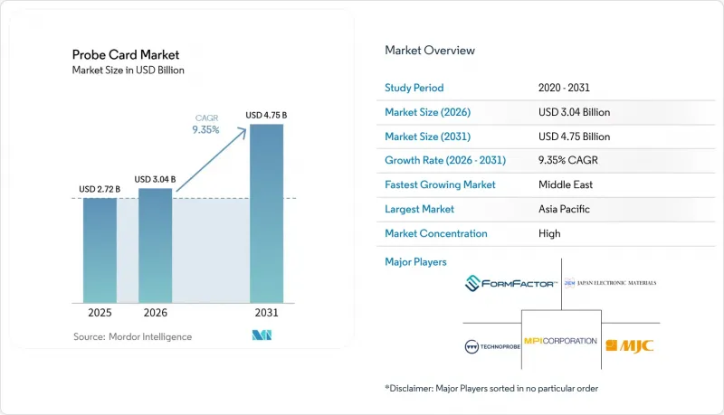
Mordor Intelligence에 의하면, 프로브 카드 시장 규모는 2025년 27억 2,000만 달러에서 2026년에는 30억 4,000만 달러로 확대되어 2031년까지 47억 5,000만 달러에 이를 것으로 예상되고 있어 2026년부터 2031년까지 CAGR 9.35%로 성장할 전망입니다.
본 보고서는 기술별(MEMS, 수직형, 캔틸레버형, 특수형), 용도별(DRAM, 플래시 메모리, 파운드리 및 로직, 파라메트릭, 기타), 유형별(표준 프로브 카드, 첨단 프로브 카드),최종 사용자(파운드리, 집적 소자 제조업체, OSAT, 연구 기관), 웨이퍼 크기(150mm 이하, 200mm, 300mm, 450mm) 및 지역별로 분류되어 있습니다. 시장 예측은 금액(달러) 기준으로 제시되어 있습니다.
세계 프로브 카드 시장 동향 및 인사이트
소비자용 전자기기 및 IoT 기기 수요 증가
2025년, 스마트폰 출하 대수는 12억 대로 보합세를 보였으나, 전용 AI 엔진과 첨단 전원 관리 IC가 견인 역할을 하여 기기당 반도체 탑재량은 18% 증가했습니다. 자동차용 전자 기기에 대한 지출은 2025년에 820억 달러에 달할 것으로 예상되며, 현재 전기차에는 1대당 최대 3,000개의 칩이 탑재되어 있습니다. IoT 도입 대수는 160억 대를 돌파했으며, 산업용 및 의료용 엔드포인트에서는 극한 온도 조건 하에서의 혼합 신호 검증이 요구되고 있습니다. 이러한 변화로 인해 프로브 카드 수요는 단순한 대수에 좌우되지 않게 되었으며, 소비자용 제품의 생산량이 정점에 달하더라도 웨이퍼 레벨 테스트 현장은 계속해서 활기를 띠고 있습니다. 2025년에 발표된 Apple의 맞춤형 M4 프로세서는 통합 메모리 아키텍처를 위한 맞춤형 프로브 솔루션을 필요로 하는 수직 통합 전략을 더욱 부각시키고 있습니다.
반도체 소자의 미세화
TSMC는 2025년 하반기에 2nm 게이트 올 어라운드(GAA) 공정의 양산으로 전환함에 따라, 패드 손상을 방지하면서 10마이크로미터 이내로 위치 결정이 가능한 프로브 칩이 필요하게 되었습니다. 인텔이 향후 도입할 18A 노드에서는 후면 전원 공급 방식이 도입됨에 따라, 기존 캔틸레버식 카드로는 대응할 수 없는 양면 프로빙이 요구되고 있습니다. 삼성의 1.4nm를 향한 로드맵에서는 5nm 공정에 비해 프로브 교체 빈도가 2배로 증가하여 웨이퍼 1장당 테스트 비용이 상승하고, 공급업체의 인증 기간이 단축되고 있습니다. 또한, 극자외선(EUV) 노광의 도입으로 인해 웨이퍼 수준의 파라메트릭 테스트에서만 감지할 수 있는 국소적인 수율 저하 요인도 발생하고 있어, 고정밀 프로브 카드에 대한 의존도가 높아지고 있습니다.
첨단 프로브 카드 개발의 높은 비용
최첨단 프로브 카드는 반복적인 프로토타이핑, 재료 과학, 다온도 검증 등을 포함해 250만 달러 이상의 비용이 소요될 수 있으며, 이러한 비용을 상각할 수 있는 곳은 최대 규모의 팹뿐입니다. 치플릿 아키텍처의 세분화로 인해 설계당 생산량이 더욱 감소하고 있어, 규모의 경제 효과가 약화되고 있습니다. 소규모 팹은 막대한 전환 비용에 직면해 있어 기존 공급업체에 얽매이게 되며, 인증 주기가 1년까지 길어지고 있습니다. 공급업체들은 클린룸 및 서브미크론 가공을 위한 막대한 설비 투자를 부담하고 있어, 최종 시장의 생산량이 증가하고 있음에도 불구하고 신규 진입을 제한하고 있습니다.
부문 분석
MEMS 설계는 10,000패드를 초과하는 접점 밀도와 5마이크로미터 미만의 위치 정확도(이것들은 게이트 올 어라운드(GAA) 공정에 필수적인 지표)로 인해 2025년 매출의 44.76%를 차지했습니다. 파운드리 업체들이 3nm 미만으로 전환하고 후면 전원 레일을 채택함에 따라, 수직형 MEMS가 가장 빠르게 성장하고 있으며 연평균 성장률(CAGR)은 10.63%로 성장을 지속하고, 있습니다. 2025년에 출시된 FormFactor사의 60마이크로미터 미만의 피치를 가진 플랫폼을 통해, 팹에서는 1mm2당 100패드를 넘는 칩렛 상호 연결 테스트가 가능해집니다. 캔틸레버 방식 카드는 저비용이라는 장점 덕분에 성숙한 노드에서 여전히 사용되고 있지만, 테스트 팀이 툴 세트를 통합함에 따라 그 점유율은 계속 하락하고 있습니다.
초기 수율은 스프링 상수의 균일성에 좌우됩니다. 수직형 MEMS는 ±5%의 편차를 유지하는 반면, 캔틸레버형은 ±20%이므로 웨이퍼 레벨 번인(burn-in) 시 접촉 신뢰성이 향상됩니다. 일본공급업체들은 초미세 피치 솔루션을 요구하는 국내 팹에 대응하기 위해 2025년에 생산 능력을 40% 확대했습니다. AI를 활용한 정렬을 통해 셋업 사이클이 30% 단축되어, MEMS 카드는 첫 접촉에서 99.5%의 접촉률을 달성할 수 있게 되었습니다. 이는 오늘날의 대량 생산 라인에서 필수적인 처리량 요건입니다. 멤브레인 카드와 같은 특수 포맷은 자동차 전동화와 관련된 RF 검증 및 파워 디바이스 프로빙에서 여전히 중요한 역할을 하고 있습니다.
2025년에는 파운드리 및 로직이 47.59%의 점유율을 차지하며 주도적인 위치를 차지했으나, 3D NAND의 적층 수가 200스택을 돌파하고 웨이퍼당 테스트 벡터 수가 증가함에 따라,플래시 메모리는 연평균 성장률(CAGR) 11.02%로 확대되고 있습니다. 삼성의 286층 V-NAND의 경우, 처리량 목표를 달성하기 위해 16개의 다이를 동시에 프로빙할 수 있는 카드가 필요했습니다. DRAM 출하량은 DDR5 기준으로 정체를 보이고 있지만, AI 서버용 고대역폭 변형 제품은 다이의 적층화를 통해 점진적인 수요를 유지하고 있습니다.
인텔의 18A 공정에서는 파라메트릭 모니터링이 웨이퍼당 15포인트로 확대되어, 로트당 카드 소비량이 7nm 기준에 비해 25% 증가했습니다. 아날로그, 혼합 신호 및 파워 디바이스는 웨이퍼 100% 스크리닝을 의무화하는 자동차 안전 기준 덕분에 호재를 누리고 있습니다. 치플렛의 보급으로 용도의 경계가 모호해지면서, 로직 속도 테스트와 고속 메모리 아이스캔을 한 번의 터치다운으로 결합한 하이브리드 카드의 개발이 촉진되고 있습니다.
지역별 분석
아시아태평양은 대만이 세계 수요의 45%를 차지하고, 한국의 메모리 분야 리더십, 그리고 일본의 국내 조달 정책에 힘입어 2025년 매출의 84.12%를 유지했습니다. 대만의 프로브 카드 생태계는 TSMC의 2nm 공정 양산 개시와 TSMC가 추진하는 400억 달러 규모의 미국 공장 건설의 혜택을 받고 있습니다. 또한 TSMC는 공정의 연속성을 확보하기 위해 여전히 국내 공급업체로부터 프로브 카드를 조달하고 있습니다. 한국의 삼성과 SK하이닉스는 2025년에 2억 5,000만 개 이상의 고대역폭 스택을 출하할 예정이며, 실리콘 관통 비아(TSV) 테스트용 특수 카드가 필요합니다. 일본 클러스터는 구마모토 팹의 현지 조달 규정에 따라 구매처가 마이크로닉스 재팬(Micronix Japan) 및 재팬 일렉트로닉 머티리얼즈(Japan Electronic Materials)로 유도됨에 따라 탄력을 받았습니다. 중국 수요는 성숙한 노드를 중심으로 확대되고 있지만, 수출 규제로 인해 최첨단 카드 설계에 대한 접근이 제한되고 있어 국내에서 기술 혁신이 추진되고 있습니다.
북미는 연평균 성장률(CAGR) 8.2%로 확대되고 있으며, 인텔, TSMC, 삼성의 ‘CHIPS법’에 기반한 팹에서는 2027년까지 3억 달러 상당의 추가 테스트용 하드웨어가 필요할 것으로 예측됩니다. 유럽은 연평균 성장률(CAGR) 7.9%로 그 뒤를 잇고 있으며, 인텔의 마그데부르크 거점, ST마이크로일렉트로닉스의 그르노블 확장, 인피니온의 드레스덴 거점 업그레이드가 진행 중이며, 이들 모두 지역적 복원력 요건을 준수하고 있습니다. 중동은 사우디아라비아와 아랍에미리트가 합작 투자 모델을 통해 28nm 이상의 생산 능력에 자금을 지원하고 있어 연평균 성장률(CAGR) 10.06%로 가장 빠른 성장 궤도를 보이고 있습니다. 남미와 아프리카는 여전히 규모가 작지만, 브라질이 2025년에 도입할 조립에 대한 세제 혜택이 향후 프로브 카드 시장의 틈새 분야를 육성할 가능성이 있습니다.
듀얼 소싱 전략은 지정학적 리스크를 완화하고, 공급업체들이 거점을 다각화하도록 촉진하고 있습니다. 폼팩터(Form Factor)는 필리핀 공장을 확장했고, 테크노프로브(Techno Probe)는 리드타임 단축을 위해 텍사스주에 서비스 허브를 개설했습니다. 라이선싱 규제 대응으로 인해 공급이 세분화되어, 성숙한 노드에서 중국 내 제조업체에 진입 기회가 열리고 있습니다. 한편, 아시아 이외 지역에서의 기술 이전 지연으로 인해 유럽 및 미국의 팹(fab)에서 인증 절차가 장기화되고 있습니다. 인텔(Intel)의 18A 라인이 TSMC의 12개월이라는 선례에 비해 18개월의 도입 주기를 소요했던 것이 그 예입니다.
기타 혜택:
- 엑셀 형식 시장 예측(ME) 시트
- 3개월간의 애널리스트 지원
자주 묻는 질문
목차
제1장 서론
제2장 조사 방법
제3장 개요
제4장 시장 구도
제5장 시장 규모와 성장 예측
제6장 경쟁 구도
제7장 시장 기회와 향후 전망
JHS 26.09.03According to Mordor Intelligence, the probe card market size is expected to increase from USD 2.72 billion in 2025 to USD 3.04 billion in 2026 and reach USD 4.75 billion by 2031, growing at a CAGR of 9.35% over 2026-2031.
This report is Segmented by Technology (MEMS, Vertical, Cantilever, and Specialty), Application (DRAM, Flash, Foundry and Logic, Parametric, and More), Type (Standard Probe Card, and Advanced Probe Card), End User (Foundries, Integrated Device Manufacturers, Osats, and Research Institutes), Wafer Size (Up To 150mm, 200mm, 300mm, and 450mm), and Geography. The Market Forecasts are Provided in Terms of Value (USD).
Global Probe Card Market Trends and Insights
Rising Demand for Consumer Electronics and IoT Devices
Smartphone shipments stabilized at 1.2 billion units in 2025, but semiconductor content per handset climbed 18%, led by dedicated AI engines and advanced power-management ICs. Automotive electronics spending reached USD 82 billion in 2025, as electric vehicles now integrate up to 3,000 chips per unit. The installed IoT base surpassed 16 billion devices, with industrial and healthcare endpoints demanding mixed-signal validation across temperature extremes. These shifts decouple probe card demand from mere unit counts, keeping wafer-level test floors busy even when consumer volume plateaus. Apple's custom M4 processors, introduced in 2025, further spotlight vertical integration strategies that require bespoke probe solutions for unified memory architectures.
Miniaturization of Semiconductor Devices
TSMC moved to volume production of its 2 nm gate-all-around process in late 2025, necessitating probe tips that position within 10 micrometers while avoiding pad damage. Intel's forthcoming 18A node introduces backside power delivery, compelling dual-sided probing that traditional cantilever cards cannot address. Samsung's roadmap toward 1.4 nm has doubled probe replacement frequency versus 5 nm processes, lifting per-wafer test costs and tightening supplier qualification windows. Extreme ultraviolet exposure has also introduced localized yield detractors detectable only through wafer-level parametric testing, intensifying the reliance on high-precision probe cards.
High Cost of Advanced Probe Card Development
A leading-edge probe card can cost more than USD 2.5 million, covering iterative prototyping, material science, and multi-temperature validation, costs that only the largest fabs can amortize. Fragmentation in chiplet architectures further erodes volumes per design, blunting scale economies. Smaller fabs face prohibitive switching expenses, locking them into incumbent suppliers and stretching qualification cycles to a year. Suppliers absorb heavy capex for cleanrooms and sub-micron machining, constraining new entrants despite rising end-market volumes.
Other drivers and restraints analyzed in the detailed report include:
- Growth in Advanced Packaging and 3D IC Technologies
- Complexity of Testing at Sub-5 nm Nodes
For complete list of drivers and restraints, kindly check the Table Of Contents.
Segment Analysis
MEMS designs captured 44.76% of 2025 revenue, owing to contact densities above 10,000 pads and positional accuracy better than 5 micrometers, metrics critical for gate-all-around processes. Vertical MEMS is the fastest mover, clocking a 10.63% CAGR as foundries migrate below 3 nm and adopt backside power rails. FormFactor's sub-60 micrometer pitch platform, launched in 2025, lets fabs probe chiplet interconnects exceeding 100 pads per mm2. Cantilever cards linger in mature nodes due to lower cost, yet their share continues to slip as test teams consolidate tooling portfolios.
First-pass yield hinges on spring-constant uniformity: vertical MEMS maintains +-5% variation versus +-20% for cantilevers, elevating contact reliability in wafer-level burn-in. Japanese suppliers expanded capacity by 40% in 2025 to serve local fabs demanding ultra-fine-pitch solutions. AI-assisted alignment shortens setup cycles by 30%, enabling MEMS cards to achieve 99.5% contact on first touchdown, a throughput imperative for today's high-volume lines. Specialty formats such as membrane cards retain relevance in RF validation and power-device probing tied to automotive electrification.
Foundry and logic dominated with 47.59% share in 2025, but flash memory is expanding at 11.02% CAGR as 3D NAND layers breach the 200-stack threshold, inflating test vectors per wafer. Samsung's 286-layer V-NAND required cards able to probe 16 dies simultaneously to hit throughput targets. DRAM unit volumes plateau around DDR5, yet high-bandwidth variants in AI servers sustain incremental demand through stacked dies.
Parametric monitoring now covers 15 points per wafer on Intel's 18A flow, lifting card consumption per lot by 25% over 7 nm baselines. Analog, mixed-signal, and power devices gain tailwinds from automotive safety norms mandating 100% wafer screening. Chiplet convergence is blurring application lines, spurring hybrid cards that combine logic speed tests with high-speed memory eye scans in one touchdown.
Complete Report Scope:
- By Technology
- MEMS
- Vertical
- Cantilever
- Specialty
- By Application
- DRAM
- Flash
- Foundry and Logic
- Parametric
- Other Applications
- By Type
- Standard Probe Card
- Advanced Probe Card
- By End User
- Foundries
- Integrated Device Manufacturers
- Outsourced Semiconductor Assembly and Test
- Research Institutes
- By Wafer Size
- 150 mm and Below
- 200 mm
- 300 mm
- 450 mm
- By Geography
- North America
- United States
- Canada
- Mexico
- South America
- Brazil
- Argentina
- Rest of South America
- Europe
- Germany
- France
- United Kingdom
- Italy
- Spain
- Russia
- Rest of Europe
- Asia-Pacific
- China
- Japan
- South Korea
- Taiwan
- India
- ASEAN
- Rest of Asia-Pacific
- Middle East
- Saudi Arabia
- United Arab Emirates
- Turkey
- Israel
- Rest of Middle East
- Africa
- South Africa
- Nigeria
- Kenya
- Egypt
- Rest of Africa
- North America
Geography Analysis
Asia Pacific retained 84.12% of 2025 revenue, anchored by Taiwan's 45% share of global demand, South Korea's memory leadership, and Japan's domestic content policies. Taiwan's probe card ecosystem benefits from TSMC's 2 nm ramp and the company's USD 40 billion U.S. build, which still sources cards from home suppliers for process continuity. South Korea's Samsung and SK Hynix shipped more than 250 million high-bandwidth stacks in 2025, needing specialty cards for through-silicon via tests. Japan's cluster gained momentum as local content rules at the Kumamoto fab steered purchases to Micronics Japan and Japan Electronic Materials. China's demand grows around mature nodes, but export controls limit access to cutting-edge card designs, prompting domestic innovation.
North America is rising at 8.2% CAGR as CHIPS Act fabs from Intel, TSMC, and Samsung require USD 300 million of incremental test hardware by 2027. Europe follows at 7.9% CAGR via Intel's Magdeburg site, STMicroelectronics' Grenoble expansion, and Infineon's Dresden upgrades, each bound by local resiliency mandates. The Middle East shows the fastest trajectory at 10.06% CAGR as Saudi Arabia and the United Arab Emirates fund 28 nm-plus capacity with joint-venture models. South America and Africa remain small, though Brazil's 2025 tax incentives for assembly could seed future probe card niches.
Dual-sourcing strategies mitigate geopolitical exposure, pushing suppliers to diversify footprints. FormFactor enlarged its Philippines plant, while Technoprobe opened a Texas service hub for faster turns. Export-license navigation fragments supply, granting domestic Chinese makers an opening in mature nodes. Meanwhile, knowledge-transfer lags outside Asia lengthen qualification for Western fabs, as Intel's 18A line illustrates with its 18-month onboarding cycle versus TSMC's 12-month precedent.
- FormFactor Inc.
- Technoprobe S.p.A.
- Micronics Japan Co. Ltd.
- Japan Electronic Materials Corporation
- MPI Corporation
- Feinmetall GmbH
- Korea Instrument Co. Ltd.
- Wentworth Laboratories Inc.
- GGB Industries Inc.
- Protec MEMS Technology
- Nidec SV Probe Pte. Ltd.
- STAr Technologies Inc.
- Willtechnology Co. Ltd.
- TSE Co. Ltd.
- Chunghwa Precision Test Tech Co. Ltd.
- Microfriend Inc.
- Synergie-Cad Probe
- TIPS Messtechnik GmbH
- MaxOne Technologies Co. Ltd.
- Shenzhen Fastprint Circuit Tech Co. Ltd.
Additional Benefits:
- The market estimate (ME) sheet in Excel format
- 3 months of analyst support
TABLE OF CONTENTS
1 INTRODUCTION
- 1.1 Study Assumptions and Market Definition
- 1.2 Scope of the Study
2 RESEARCH METHODOLOGY
3 EXECUTIVE SUMMARY
4 MARKET LANDSCAPE
- 4.1 Market Overview
- 4.2 Market Drivers
- 4.2.1 Rising Demand for Consumer Electronics and IoT Devices
- 4.2.2 Miniaturization of Semiconductor Devices
- 4.2.3 Growth in Advanced Packaging and 3D IC Technologies
- 4.2.4 Momentum in Foundry Expansion Incentive Programs
- 4.2.5 Shift Toward Less than 60 µm Vertical MEMS Probe Cards
- 4.2.6 Adoption of AI-Assisted Probe Card Alignment Systems
- 4.3 Market Restraints
- 4.3.1 High Cost of Advanced Probe Card Development
- 4.3.2 Complexity of Testing at Sub-5 nm Nodes
- 4.3.3 Cyclical Nature of Semiconductor Capital Expenditure
- 4.3.4 Limited Availability of Ultra-Low-Resistance Probe Materials
- 4.4 Industry Value Chain Analysis
- 4.5 Regulatory Landscape
- 4.6 Technological Outlook
- 4.7 Porter's Five Forces Analysis
- 4.7.1 Bargaining Power of Suppliers
- 4.7.2 Bargaining Power of Buyers
- 4.7.3 Threat of New Entrants
- 4.7.4 Threat of Substitutes
- 4.7.5 Intensity of Competitive Rivalry
- 4.8 Pricing Trend Analysis
- 4.9 Analysis of RF Probe Cards
5 MARKET SIZE AND GROWTH FORECASTS (VALUE)
- 5.1 By Technology
- 5.1.1 MEMS
- 5.1.2 Vertical
- 5.1.3 Cantilever
- 5.1.4 Specialty
- 5.2 By Application
- 5.2.1 DRAM
- 5.2.2 Flash
- 5.2.3 Foundry and Logic
- 5.2.4 Parametric
- 5.2.5 Other Applications
- 5.3 By Type
- 5.3.1 Standard Probe Card
- 5.3.2 Advanced Probe Card
- 5.4 By End User
- 5.4.1 Foundries
- 5.4.2 Integrated Device Manufacturers
- 5.4.3 Outsourced Semiconductor Assembly and Test
- 5.4.4 Research Institutes
- 5.5 By Wafer Size
- 5.5.1 150 mm and Below
- 5.5.2 200 mm
- 5.5.3 300 mm
- 5.5.4 450 mm
- 5.6 By Geography
- 5.6.1 North America
- 5.6.1.1 United States
- 5.6.1.2 Canada
- 5.6.1.3 Mexico
- 5.6.2 South America
- 5.6.2.1 Brazil
- 5.6.2.2 Argentina
- 5.6.2.3 Rest of South America
- 5.6.3 Europe
- 5.6.3.1 Germany
- 5.6.3.2 France
- 5.6.3.3 United Kingdom
- 5.6.3.4 Italy
- 5.6.3.5 Spain
- 5.6.3.6 Russia
- 5.6.3.7 Rest of Europe
- 5.6.4 Asia-Pacific
- 5.6.4.1 China
- 5.6.4.2 Japan
- 5.6.4.3 South Korea
- 5.6.4.4 Taiwan
- 5.6.4.5 India
- 5.6.4.6 ASEAN
- 5.6.4.7 Rest of Asia-Pacific
- 5.6.5 Middle East
- 5.6.5.1 Saudi Arabia
- 5.6.5.2 United Arab Emirates
- 5.6.5.3 Turkey
- 5.6.5.4 Israel
- 5.6.5.5 Rest of Middle East
- 5.6.6 Africa
- 5.6.6.1 South Africa
- 5.6.6.2 Nigeria
- 5.6.6.3 Kenya
- 5.6.6.4 Egypt
- 5.6.6.5 Rest of Africa
- 5.6.1 North America
6 COMPETITIVE LANDSCAPE
- 6.1 Market Concentration
- 6.2 Strategic Moves
- 6.3 Market Share Analysis
- 6.4 Company Profiles (includes Global level Overview, Market level Overview, Core Segments, Financials as available, Strategic Information, Market Rank/Share for key companies, Products and Services, and Recent Developments)
- 6.4.1 FormFactor Inc.
- 6.4.2 Technoprobe S.p.A.
- 6.4.3 Micronics Japan Co. Ltd.
- 6.4.4 Japan Electronic Materials Corporation
- 6.4.5 MPI Corporation
- 6.4.6 Feinmetall GmbH
- 6.4.7 Korea Instrument Co. Ltd.
- 6.4.8 Wentworth Laboratories Inc.
- 6.4.9 GGB Industries Inc.
- 6.4.10 Protec MEMS Technology
- 6.4.11 Nidec SV Probe Pte. Ltd.
- 6.4.12 STAr Technologies Inc.
- 6.4.13 Willtechnology Co. Ltd.
- 6.4.14 TSE Co. Ltd.
- 6.4.15 Chunghwa Precision Test Tech Co. Ltd.
- 6.4.16 Microfriend Inc.
- 6.4.17 Synergie-Cad Probe
- 6.4.18 TIPS Messtechnik GmbH
- 6.4.19 MaxOne Technologies Co. Ltd.
- 6.4.20 Shenzhen Fastprint Circuit Tech Co. Ltd.
7 MARKET OPPORTUNITIES AND FUTURE OUTLOOK
- 7.1 White-Space and Unmet-Need Assessment


