|
시장보고서
상품코드
2121339
이미지 센서 : 시장 점유율 분석, 업계 동향과 통계, 성장 예측(2026-2031년)Image Sensors - Market Share Analysis, Industry Trends & Statistics, Growth Forecasts (2026 - 2031) |
||||||
 Mordor Intelligence
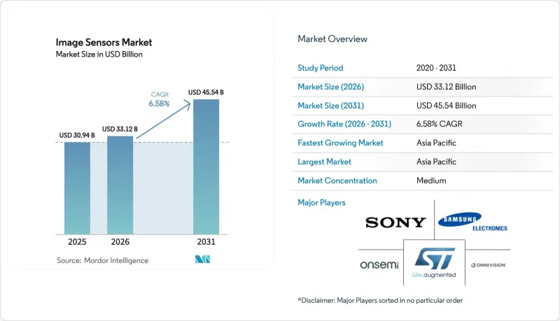
Mordor Intelligence에 따르면 이미지 센서 시장 규모는 2025년 309억 4,000만 달러에서 2026년에는 331억 2,000만 달러로 확대되어 2031년까지 455억 4,000만 달러에 달할 것으로 예측되며, 2026년부터 2031년까지 CAGR 6.58%로 성장할 것으로 전망됩니다.
본 보고서는 유형별(CMOS 및 CCD), 처리 기술별(표면 조사형(FSI), 후면 조사형(BSI), 적층형 BSI), 셔터 유형별(롤링 셔터, 세계 셔터), 스펙트럼별(가시광선(RGB), 근적외선(NIR), 단파장 적외선(SWIR), X선·자외선), 해상도별(1MP 미만, 1-3MP, 4-12MP, 13-24MP, 25MP 이상), 최종사용자 산업별(가정용 전자기기, 자동차·운송 산업, 산업용 자동화·로봇, 보안 모니터링, 기타), 지역별로 분류되어 있습니다. 시장 전망은 금액(달러) 기준으로 제시되어 있습니다.
세계 이미지 센서 시장의 동향 및 인사이트
스마트폰의 멀티 카메라 보급이 CMOS 수요를 끌어올리면서
2025년, 전 세계 휴대전화 제조사들은 후면 카메라 3개 이상을 탑재한 스마트폰을 12억 대 출하하여 전년 대비 26% 증가했습니다. 이는 중저가 모델에서 과거에는 플래그십 모델에만 한정되었던 초광각 및 망원 모듈이 채택되었기 때문입니다. 경쟁 압력으로 인해 부품 원가가 압박받으면서, 센서 공급업체들은 평균 판매 가격 하락을 감수하면서도 막대한 생산량에 연구 개발을 분산할 수밖에 없게 되었습니다. 소니나 삼성처럼 자체 웨이퍼 제조 능력과 이미지 신호 프로세서(ISP) 코어를 보유한 수직 통합형 기업은 수익성을 유지할 수 있는 입장에 있습니다. 컴퓨테이셔널 포토그래피의 발전으로 가치의 중심은 광학 시스템에서 화소로 더욱 이동하고 있습니다. 애플의 ‘딥 퓨전(Deep Fusion)’이나 구글의 ‘나이트 사이트(Night Sight)’와 같은 알고리즘은 높은 다이나믹 레인지와 낮은 판독 노이즈에 의존하고 있어, 120dB의 다이나믹 레인지를 실현하는 온칩 14비트 컨버터를 탑재한 적층형 BSI 칩이 특히 중요시되고 있습니다.
레벨 3 이상의 ADAS를 구현하는 자동차용 세계 셔터 센서
차량의 주행 속도가 100km/h를 초과하면 롤링 셔터로 인한 아티팩트가 용납될 수 없기 때문에 각 OEM 업체들은 전방 카메라 및 서라운드 뷰 카메라용으로 세계 셔터 CMOS로의 전환을 추진하고 있습니다. 메르세데스-벤츠는 2024년, 8개의 세계 셔터 디바이스를 사용하여 독일과 캘리포니아주에서 ‘Drive Pilot Level 3’ 인증을 획득했습니다. ON Semiconductor의 Hyperlux 플랫폼은 3마이크로미터 픽셀과 140dB의 다이나믹 레인지를 통합하여, 대비가 높은 장면에서도 세부 사항을 충실하게 재현합니다. Euro NCAP의 2025년 테스트 프로토콜에서는 사실상 모든 모델에 보행자 감지 카메라 탑재가 의무화되어 있어, 세계 셔터의 보급을 가속화하고 있습니다.
300mm CIS 웨이퍼 생산능력 병목 현상으로 인한 가격 변동
2025년, 이미지 센서 생산에는 월간 18만 장의 300mm 웨이퍼가 소비되었으나, 수요가 공급을 8% 상회함에 따라 2025년 초 자동차용 센서 가격이 12% 상승했습니다. 소니는 구마모토 공장의 생산능력을월 4만 장 분량으로 확대하기 위해 2,000억 엔(13억 4,000만 달러)을 투자했으나, 이 추가 생산능력이 가동되는 것은 2026년 말이 되어서야 가능합니다. 장기 계약을 체결하지 않은 팹리스 벤더들은 16주간의 리드타임과 이익률 압박에 직면해 있습니다.
부문별 분석
CMOS 디바이스는 2025년 매출의 93.17%를 차지하며, 그 점유율은 규모의 경제를 확고히 하고, 전하 결합 소자(CCD)에 대한 이미지 센서의 시장 점유율 우위를 이끌고 있습니다. CMOS는 판독 회로, A/D 변환기, 심지어 신경망 가속기까지 동일한 다이 위에 집적하여 조립 비용을 30% 절감하고, 소비 전력을 500mW 이하로 억제하고 있습니다. CCD는 천문학, 병리학, 의료용 내시경 부문에서 6.83%의 점유율을 차지하고 있으며, 이러한 부문에서는 프레임 속도가 낮다는 단점을 상쇄하는, 1전자 미만의 판독 노이즈가 높이 평가되고 있습니다. Sony의 IMX661로 대표되는 과학용 CMOS는 현재 95%의 양자 효율과 0.3e- 이하의 판독 노이즈를 실현하고 있어, CCD의 틈새 시장을 잠식하고 있습니다. 단파장 적외선(SWIR) CMOS는 현재로서는 극히 일부에 불과하지만, 산업용 및 농업용 애플리케이션이 실리콘 CCD에서 인듐-갈륨-비소(InGaAs) 포토다이오드로 전환됨에 따라 연간 7.11%의 속도로 확대되고 있습니다.
CCD는 암전류를 최소화하면서 10시간의 적분 촬영을 목표로 하는 심우주 관측소에서 여전히 최적의 선택지입니다. 의료용 이미징 기업들은 색상을 충실하게 재현하여 조직을 식별할 수 있는 CCD의 균일성을 높이 평가하고 있습니다. 그러나 과학 기기용 이미지 센서 시장의 규모가 노이즈 0.5e- 이하의 적층형 BSI CMOS로 전환됨에 따라 CCD의 출하량은 감소할 것으로 예측됩니다. 틈새 시장 공급업체들은 맞춤형 생산을 통해 살아남겠지만, 주류인 휴대전화, 자동차, 비전 시스템 구매자들은 첨단 CMOS 공급망을 중심으로 통합이 진행될 것으로 보입니다.
2025년에는 후면 조사형 기술이 매출의 44.68%를 차지했습니다. 그러나 각 벤더들이 포토다이오드 아래에 DRAM(동적 랜덤 액세스 메모리)과 AI 코어를 내장하여 센서를 초저지연 프로세서로 변모시킴에 따라, 적층형 BSI는 7.34%의 성장률을 보이고 있습니다. 소니의 IMX989는 28nm 로직 다이 위에 45nm 화소 어레이를 적층하여, 이미지에서 디스플레이로 전송되는 지연 시간을 50ms에서 5ms로 단축하고 14비트 HDR 촬영을 가능하게 합니다. 표면 조사형 CMOS는 여전히 가격에 민감한 후방 카메라에 채택되고 있으며, 이 경우 15%의 부품 비용 절감이 40%의 감도 저하를 상쇄하고 있습니다.
이종 통합 기술이 성숙해짐에 따라, 적층형 BSI와 관련된 이미지 센서 시장의 규모는 계속 확대될 것으로 보입니다. 캐논의 실온 표면 활성화 본딩 기술은 자동차 산업의 결함 허용 기준을 충족하면서도 BSI의 수율을 12포인트 향상시킵니다. 실리콘 관통 비아(TSV) 형성으로 인해 공정이 늘어나 비용이 8% 증가하지만, 각 OEM 업체들은 10mm 사방의 모듈 내에서 실현되는 다중 노출 HDR, 프레임별 AI 추론, 렌즈 수차 보정의 이점을 위해 이 추가 비용을 감수하고 있습니다.
지역별 분석
아시아태평양은 2025년 매출의 44.21%를 차지하며, 2031년까지 연평균 성장률(CAGR) 7.65%로 성장할 것으로 예측됩니다. 중국은 스마트폰의 68%, 보안 카메라의 52%를 조립하고 있으며, 수출 규제라는 역풍에도 불구하고 현지 센서 제조업체들은 홈그라운드에서 우위를 점하고 있습니다. 일본의 소니와 캐논은 적층형 BSI 및 과학용 CMOS를 통해 전 세계 프리미엄 매출의 절반을 계속 차지하고 있는 반면, 한국의 삼성은 LPDDR5 메모리의 적층 기술을 활용하여 8K 녹화의 장벽을 허물었습니다.
유럽과 북미는 매출의 38%를 차지했습니다. 2024년 7월에 발효되는 유럽연합(EU)의 일반 안전 규정(GSR)에서는 자동 긴급 제동 및 차선 유지 보조 기능이 의무화되어, 이에 따라 카메라 탑재 대수가 증가하고 있습니다. STMicroelectronics와 ams OSRAM은 -40℃에서 +105℃의 온도 범위에서 작동하는 AEC-Q100 준수 센서를 공급하며, 유럽에서 탄탄한 사업 기반을 구축하고 있습니다. 북미 시장에서는 테슬라의 12개 카메라가 탑재된 ‘완전 자율주행’ 시스템과 아마존의 5만 대 비전 유도 로봇이 시장의 주도권을 양분하고 있습니다.
중동 및 아프리카, 남미가 나머지 18%를 차지했습니다. 두바이, 리야드, 도하에서는 스마트 시티용 엣지 비전이 도입되었으며, 사우디아라비아의 NEOM은 3억 달러 상당의 AI 카메라 10만 대를 발주했습니다. 남아프리카의 광산에서는 자율주행 운반 트럭에 열화상 카메라를 도입했으며, 브라질의 농업 분야에서는 SWIR(단파 적외선) 대응 관개 시스템을 검사 및 도입했습니다. 인프라 제약과 환율 변동이 급속한 보급을 저해하고 있지만, 프로젝트 기반의 수요 급증으로 인해 지역에 따라 수요가 정점을 찍고 있습니다.
기타 혜택
- 엑셀 형식의 시장 예측(ME) 시트
- 3개월간의 애널리스트 지원
자주 묻는 질문
목차
제1장 소개
제2장 조사 방법
제3장 주요 요약
제4장 시장 구도
제5장 시장 규모와 성장 예측
제6장 경쟁 구도
제7장 시장 기회와 향후 전망
KSM 26.09.03According to Mordor Intelligence, the image sensors market size is expected to increase from USD 30.94 billion in 2025 to USD 33.12 billion in 2026 and reach USD 45.54 billion by 2031, growing at a CAGR of 6.58% over 2026-2031.
This report is Segmented by Type (CMOS, and CCD), Processing Technology (FSI, BSI, and Stacked BSI), Shutter Type (Rolling, and Global), Spectrum (Visible, NIR, SWIR, and X-ray/UV), Resolution (Less Than 1 MP, 1-3 MP, 4-12 MP, 13-24 MP, and >=25 MP), End-User (Consumer Electronics, Automotive, Industrial, Security, Healthcare, and More), and Geography. Market Forecasts are Provided in Terms of Value (USD).
Global Image Sensors Market Trends and Insights
Smartphone Multicamera Proliferation Elevating CMOS Demand
Global handset vendors shipped 1.2 billion smartphones with three or more rear cameras in 2025, up 26% year-on-year, as mid-tier models adopted ultra-wide and telephoto modules once reserved for flagships. Competitive pressure compressed the bill of materials, forcing sensor suppliers to spread R&D across massive volumes while conceding lower average selling prices. Vertically integrated players such as Sony and Samsung, with captive wafer capacity and image-signal-processor (ISP) cores, are positioned to sustain profitability. Computational photography further shifts value from optics to pixels; algorithms like Apple Deep Fusion and Google Night Sight rely on high dynamic range and low read noise, placing a premium on stacked BSI chips with on-chip 14-bit converters that deliver 120 dB dynamic range.
Automotive-Grade Global-Shutter Sensors Enabling Level 3+ ADAS
Rolling-shutter artifacts become unacceptable when vehicles travel above 100 km/h, prompting OEMs to switch to global-shutter CMOS for forward-facing and surround-view cameras. Mercedes-Benz certified Drive Pilot Level 3 in Germany and California in 2024 using eight global-shutter devices. ON Semiconductor's Hyperlux platform integrates 3 µm pixels with 140 dB dynamic range, preserving detail in high-contrast scenes. Euro NCAP's 2025 test protocols effectively require pedestrian-detection cameras on all models, accelerating global-shutter penetration.
300 mm CIS Wafer Capacity Bottlenecks Creating Price Volatility
Image sensors consumed 180,000 300 mm wafer starts per month in 2025, yet demand exceeded supply by 8%, inflating automotive-grade sensor prices by 12% in early 2025. Sony allocated JPY 200 billion (USD 1.34 billion) to expand its Kumamoto fab by 40,000 wafers per month, but the additional capacity arrives only in late 2026. Fabless vendors lacking long-term contracts face 16-week lead times and margin pressure.
Other drivers and restraints analyzed in the detailed report include:
- Edge-AI Vision Modules Catalysing Smart-City Investments
- SWIR Sensors Penetrating Precision Agriculture and Industrial QC
- Thermal Noise Limits in Sub-1 µm Pixels Hindering Resolution Race
For complete list of drivers and restraints, kindly check the Table Of Contents.
Segment Analysis
CMOS devices captured 93.17% of 2025 revenue, a footprint that cements scale economies and drives the image sensors market share advantage over charge-coupled devices (CCD). CMOS integrates readout, analog-to-digital converters, and even neural accelerators on the same die, trimming assembly cost by 30% and power budgets below 500 mW. CCD held 6.83% share in astronomy, pathology, and medical endoscopy, where its sub-electron read noise outweighs slower frame rates. Scientific CMOS, typified by Sony's IMX661, now delivers 95% quantum efficiency and read noise under 0.3 e-, eroding CCD's niche. SWIR CMOS, while a small subset today, is expanding 7.11% per year as industrial and agricultural applications migrate from silicon CCD to indium-gallium-arsenide photodiodes.
CCD remains the tool of choice for deep-sky observatories seeking 10-hour integrations with minimal dark current. Medical imaging firms prize CCD uniformity for colour-true tissue differentiation. Yet as the image sensors market size for scientific devices shifts to stacked BSI CMOS with sub-0.5 e- noise, CCD volume is forecast to contract. Niche suppliers will survive on bespoke runs, but mainstream handset, automotive, and vision-system buyers will consolidate around advanced CMOS supply chains.
Backside-illuminated technologies owned 44.68% of revenue in 2025. However, stacked BSI is advancing at 7.34% as vendors embed dynamic random-access memory (DRAM) and AI cores under the photodiodes, converting sensors into ultra-low-latency processors. Sony's IMX989 stacks a 45 nm pixel array atop a 28 nm logic die, cutting image-to-display latency from 50 ms to 5 ms and enabling 14-bit HDR capture. Front-side-illuminated CMOS remains in price-sensitive rear-view cameras, where a 15% bill-of-materials saving still outweighs the 40% sensitivity penalty.
The image sensors market size linked to stacked BSI will keep expanding as heterogeneous integration matures. Canon's room-temperature surface-activated bonding raises BSI yields by 12 points while meeting automotive defect thresholds. Although through-silicon-via formation adds process steps and 8% cost, OEMs accept the premium for multi-exposure HDR, per-frame AI inference, and lens aberration correction delivered within a 10 mm-square module.
Complete Report Scope:
- By Type
- CMOS
- CCD
- By Processing Technology
- Front-Side Illuminated (FSI)
- Back-Side Illuminated (BSI)
- Stacked BSI
- By Shutter Type
- Rolling Shutter
- Global Shutter
- By Spectrum
- Visible (RGB)
- Near-Infrared (NIR)
- Short-Wave Infrared (SWIR)
- X-ray / Ultraviolet
- By Resolution
- Less than 1 MP
- 1 - 3 MP
- 4 - 12 MP
- 13 - 24 MP
- More than Equal to 25 MP
- By End-User Industry
- Consumer Electronics
- Automotive and Transportation
- Industrial Automation and Robotics
- Security and Surveillance
- Healthcare and Life Sciences
- Aerospace and Defense
- Smart City, Agriculture, Marine
- By Geography
- North America
- United States
- Canada
- Mexico
- Europe
- United Kingdom
- Germany
- France
- Italy
- Rest of Europe
- Asia-Pacific
- China
- Japan
- India
- South Korea
- Rest of Asia-Pacific
- Middle East
- Israel
- Saudi Arabia
- United Arab Emirates
- Turkey
- Rest of Middle East
- Africa
- South Africa
- Egypt
- Rest of Africa
- South America
- Brazil
- Argentina
- Rest of South America
- North America
Geography Analysis
Asia-Pacific contributed 44.21% of 2025 revenue and is projected to grow 7.65% CAGR to 2031. China assembled 68% of smartphones and 52% of security cameras, giving local sensor firms a home-field advantage despite export-control headwinds. Japan's Sony and Canon retained half of global premium revenue from stacked BSI and scientific CMOS, while South Korea's Samsung leveraged LPDDR5 memory stacking to break 8K recording barriers.
Europe and North America pooled 38% of revenue. The European Union's General Safety Regulation, effective July 2024, mandates automated emergency braking and lane-keeping assist, lifting camera content. STMicroelectronics and ams OSRAM supply AEC-Q100 sensors that operate from -40 °C to +105 °C, anchoring a defensible European franchise. North American momentum splits between Tesla's 12-camera Full Self-Driving suite and Amazon's 50,000 vision-guided robots.
The Middle East, Africa, and South America captured the remaining 18%. Dubai, Riyadh, and Doha rolled out smart-city edge vision, while Saudi Arabia's NEOM ordered 100,000 AI cameras worth USD 300 million. South Africa's mines deployed thermal imagers on autonomous haul trucks, and Brazil's agribusiness tested SWIR-enabled irrigation. Infrastructure constraints and foreign-exchange volatility temper accelerated uptake, but project-based spikes create localized demand peaks.
- Sony Group Corp.
- Samsung Electronics Co., Ltd.
- OmniVision Technologies, Inc.
- STMicroelectronics N.V.
- ON Semiconductor Corporation
- Canon Inc.
- Panasonic Holdings Corporation
- Teledyne DALSA Inc.
- ams OSRAM AG
- SK hynix Inc.
- GalaxyCore Inc.
- Hamamatsu Photonics K.K.
- SmartSens Technology
- PixArt Imaging Inc.
- Himax Technologies, Inc.
- Tower Semiconductor Ltd.
- Teledyne e2v
- Gpixel Inc.
- Forza Silicon Corp.
- Toshiba Electronic Devices and Storage Corp.
- Pyxalis S.A.
Additional Benefits:
- The market estimate (ME) sheet in Excel format
- 3 months of analyst support
TABLE OF CONTENTS
1 INTRODUCTION
- 1.1 Study Assumptions and Market Definition
- 1.2 Scope of the Study
2 RESEARCH METHODOLOGY
3 EXECUTIVE SUMMARY
4 MARKET LANDSCAPE
- 4.1 Market Overview
- 4.2 Market Drivers
- 4.2.1 Smartphone Multicamera Proliferation Elevating CMOS Demand
- 4.2.2 Automotive-Grade Global-Shutter Sensors Enabling Level-3+ ADAS
- 4.2.3 Edge-AI Vision Modules Catalysing Smart-City Investments
- 4.2.4 SWIR Sensors Penetrating Precision-Agriculture And Industrial QC
- 4.2.5 3D/Event-Based Sensors Powering Next-Gen AR/VR Wearables
- 4.2.6 Government Safety Mandates Driving In-Cabin DMS Cameras
- 4.3 Market Restraints
- 4.3.1 300 mm CIS Wafer Capacity Bottlenecks Creating Price Volatility
- 4.3.2 Thermal Noise Limits in Sub-1 µm Pixels Hindering Resolution Race
- 4.3.3 Export Controls on Advanced Imaging Chips Impacting Chinese OEMs
- 4.3.4 High Integration Cost of SWIR Sensors Slowing Consumer Uptake
- 4.4 Industry Value-Chain Analysis
- 4.5 Regulatory Outlook
- 4.6 Technological Outlook
- 4.7 Porter's Five Forces Analysis
- 4.7.1 Bargaining Power of Suppliers
- 4.7.2 Bargaining Power of Consumers
- 4.7.3 Threat of New Entrants
- 4.7.4 Threat of Substitutes
- 4.7.5 Intensity of Competitive Rivalry
- 4.8 Impact of Macroeconomic Factors on the Market
5 MARKET SIZE AND GROWTH FORECASTS (VALUE)
- 5.1 By Type
- 5.1.1 CMOS
- 5.1.2 CCD
- 5.2 By Processing Technology
- 5.2.1 Front-Side Illuminated (FSI)
- 5.2.2 Back-Side Illuminated (BSI)
- 5.2.3 Stacked BSI
- 5.3 By Shutter Type
- 5.3.1 Rolling Shutter
- 5.3.2 Global Shutter
- 5.4 By Spectrum
- 5.4.1 Visible (RGB)
- 5.4.2 Near-Infrared (NIR)
- 5.4.3 Short-Wave Infrared (SWIR)
- 5.4.4 X-ray / Ultraviolet
- 5.5 By Resolution
- 5.5.1 Less than 1 MP
- 5.5.2 1 - 3 MP
- 5.5.3 4 - 12 MP
- 5.5.4 13 - 24 MP
- 5.5.5 More than Equal to 25 MP
- 5.6 By End-User Industry
- 5.6.1 Consumer Electronics
- 5.6.2 Automotive and Transportation
- 5.6.3 Industrial Automation and Robotics
- 5.6.4 Security and Surveillance
- 5.6.5 Healthcare and Life Sciences
- 5.6.6 Aerospace and Defense
- 5.6.7 Smart City, Agriculture, Marine
- 5.7 By Geography
- 5.7.1 North America
- 5.7.1.1 United States
- 5.7.1.2 Canada
- 5.7.1.3 Mexico
- 5.7.2 Europe
- 5.7.2.1 United Kingdom
- 5.7.2.2 Germany
- 5.7.2.3 France
- 5.7.2.4 Italy
- 5.7.2.5 Rest of Europe
- 5.7.3 Asia-Pacific
- 5.7.3.1 China
- 5.7.3.2 Japan
- 5.7.3.3 India
- 5.7.3.4 South Korea
- 5.7.3.5 Rest of Asia-Pacific
- 5.7.4 Middle East
- 5.7.4.1 Israel
- 5.7.4.2 Saudi Arabia
- 5.7.4.3 United Arab Emirates
- 5.7.4.4 Turkey
- 5.7.4.5 Rest of Middle East
- 5.7.5 Africa
- 5.7.5.1 South Africa
- 5.7.5.2 Egypt
- 5.7.5.3 Rest of Africa
- 5.7.6 South America
- 5.7.6.1 Brazil
- 5.7.6.2 Argentina
- 5.7.6.3 Rest of South America
- 5.7.1 North America
6 COMPETITIVE LANDSCAPE
- 6.1 Market Concentration
- 6.2 Strategic Moves
- 6.3 Market Share Analysis
- 6.4 Company Profiles (includes Global Level Overview, Market Level Overview, Core Segments, Financials as available, Strategic Information, Market Rank/Share, Products and Services, Recent Developments)
- 6.4.1 Sony Group Corp.
- 6.4.2 Samsung Electronics Co., Ltd.
- 6.4.3 OmniVision Technologies, Inc.
- 6.4.4 STMicroelectronics N.V.
- 6.4.5 ON Semiconductor Corporation
- 6.4.6 Canon Inc.
- 6.4.7 Panasonic Holdings Corporation
- 6.4.8 Teledyne DALSA Inc.
- 6.4.9 ams OSRAM AG
- 6.4.10 SK hynix Inc.
- 6.4.11 GalaxyCore Inc.
- 6.4.12 Hamamatsu Photonics K.K.
- 6.4.13 SmartSens Technology
- 6.4.14 PixArt Imaging Inc.
- 6.4.15 Himax Technologies, Inc.
- 6.4.16 Tower Semiconductor Ltd.
- 6.4.17 Teledyne e2v
- 6.4.18 Gpixel Inc.
- 6.4.19 Forza Silicon Corp.
- 6.4.20 Toshiba Electronic Devices and Storage Corp.
- 6.4.21 Pyxalis S.A.
7 MARKET OPPORTUNITIES AND FUTURE OUTLOOK
- 7.1 White-Space and Unmet-Need Assessment