

|
시장보고서
상품코드
2122045
나노 방사선 센서 : 시장 점유율 분석, 업계 동향과 통계, 성장 예측(2026-2031년)Nano Radiation Sensors - Market Share Analysis, Industry Trends & Statistics, Growth Forecasts (2026 - 2031) |
||||||
 Mordor Intelligence
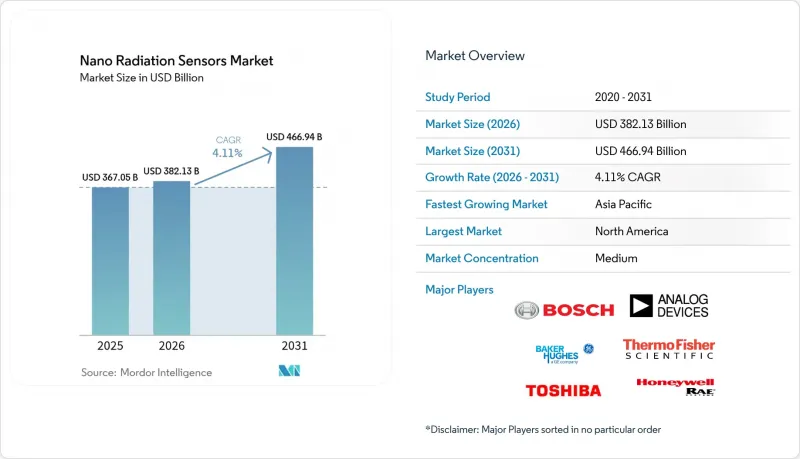
Mordor Intelligence에 의하면, 나노 방사선 센서 시장 규모는 2025년 3,670억 5,000만 달러에서 2026년에는 3,821억 3,000만 달러에 이르고, 2026-2031년 CAGR 4.11%로 성장을 지속하여 2031년에는 4,669억 4,000만 달러에 달할 것으로 예측됩니다.
본 보고서는 유형별(신틸레이션 검출기, 고체 검출기), 소재별(실리콘계 반도체, 무기 결정(GAGG, LSO, Csi) 등), 용도별(자동차, 소비자용 전자기기 등), 기술별(간접 신틸레이션·CMOS 등),검출 방사선 유형, 폼 팩터 및 지역별로 분류되어 있습니다. 시장 예측은 금액(달러) 기준으로 제시되어 있습니다.
세계 나노 방사선 센서 시장 동향 및 인사이트
업계 전반의 소형화 동향
소비자용 전자기기 및 자동차 플랫폼에서 끊임없이 진행되는 소형화 추세에 따라, 방사선 센서 모듈은 웨이퍼 레벨에서의 집적화를 향해 나아가고 있습니다. 샤프는 소비 전력이 불과 7.5 mW인 25×20×2.5 mm 모듈을 선보이며, 스마트폰을 활용한 방사선 추적의 실용화를 가능하게 했습니다. 5nm 및 3nm 공정 노드에서의 병행적인 발전으로 인해, 로직 회로와 검출 회로가 공통의 다이를 공유할 수 있게 되어 OEM 제조업체의 부품 원가가 절감되고 있습니다. 자동차 분야에서는 소형 센서가 기존 전자 제어 장치(ECU) 내에 장착될 수 있게 되어, 차량 내부를 변경하지 않고도 첨단 운전자 보조 시스템(ADAS)을 지원할 수 있게 되었습니다. IoT 아키텍처의 보급에 따라, 5년 전에는 실현 불가능했던 노드 수준의 비용으로 공장이나 병원에 분산형 나노 방사선 센서를 도입할 수 있게 되었습니다.
정부의 나노기술 자금 지원 및 규격
에 초점을 맞춘 공공 프로그램은 인증의 조화를 도모하면서 장기적인 수요를 보장하고 있습니다. 미국 상무부는 아날로그 디바이스(Analog Devices)사가 국내 3곳의 팹을 현대화하기 위해 1억 500만 달러를 배정하고, 상업용 및 방위용 방사선 감지를 우선적인 성과로 명시적으로 꼽았습니다. 영국 원자력 해체청(NDA)은 노후 원자로의 안전한 해체를 지원하기 위해 센서 연구개발에 3,000만 파운드를 투자했습니다. 이와 병행하여 유럽연합 집행위원회의 ‘호라이즌 유럽’ 플랫폼은 지속 가능한 방사선 방호 기술을 위해 자원을 투입하고 있습니다. 현재 ISO 및 IEEE 작업반은 규정 준수 주기를 단축하고 국경을 초월한 조달을 가능하게 하는 통합 나노센서 시험 프로토콜 초안을 작성하고 있습니다.
제조 복잡성 증가와 수율 저하
최신 검출기 아키텍처에 필요한 10nm 미만의 미세 구조는 주류 로직 칩보다 결함률이 높으며, 일부 파운드리에서는 초기 수율이 60% 미만에 그치고 있습니다. 포토 리소그래피용 마스크 블랭크에 고순도 실리카를 공급하는 스프루스파인 석영 광산의 일시적 폐쇄 등, 공급망의 혼란은 중요 소재공급을 위축시켜 비용 압박을 가중시키고 있습니다. 팹 운영사는 더욱 엄격한 미립자 관리와 첨단 계측 기술을 도입할 수밖에 없으며, 단기적으로는 웨이퍼당 운영 비용을 상승시킬 것입니다.
부문 분석
나노 방사선 센서 시장에서 2025년 매출의 57.35%를 고체 검출기가 차지했습니다. 이는 CMOS와의 호환성을 활용하여 감지 소자를 혼합 신호 칩에 직접 통합할 수 있게 되었기 때문입니다. 이 아키텍처는 전력 소비를 줄이고 기판 레이아웃을 단순화하며, 이러한 특징은 의료용 영상 진단 장비 및 위성 페이로드에서 높이 평가받고 있습니다. 신틸레이션 유닛은 시장 점유율은 작지만, 1 MeV당 10만 광자를 초과하는 광수율을 실현하는 페로브스카이트 나노결정 기술의 획기적인 발전에 힘입어 연평균 성장률(CAGR) 6.32%가 예상됩니다. 현재 하이브리드 설계에서는 솔리드 스테이트 판독과 나노결정 신틸레이터를 융합하여 웨이퍼 수준의 가공 비용 효율성을 유지하면서 400 ps 미만의 응답 시간을 달성하고 있습니다. 2세대 고체 플랫폼에서는 나노 플라즈모닉 증강층을 채택하여 설치 면적을 확대하지 않고도 광자 수집 효율을 3배로 높였습니다. 페로브스카이트 코팅 기술이 성숙해짐에 따라, 각 제조업체들은 실리콘 포토다이오드 위에 고-Z 신틸레이터를 모노리식 방식으로 집적하는 실험을 진행하고 있으며, 내시경 수술용 단일 칩 감마 카메라의 실현이 시야에 들어오고 있습니다. 이러한 진화는 고체 방식과 신틸레이션 방식 사이의 명확한 경계가 모호해지고, 나노 방사선 센서 업계 전체에 새로운 수익원을 창출할 것임을 시사합니다.
실리콘은 2025년 매출의 45.20%를 계속 차지할 것으로 보이며, 신뢰할 수 있는 공급과 광범위한 파운드리 지원을 제공함으로써 주류 응용 분야에서 현재 나노 방사선 센서 시장 규모를 뒷받침하고 있습니다. 생산 학습 곡선으로 인해 평균 판매 가격은 예측 가능하며, 이는 10년에 걸친 제품 주기를 다루는 자동차 업계의 1차 공급업체에게 필수적인 특성입니다. 페로브스카이트 검출기는 연평균 성장률(CAGR) 8.05%로 성장을 지속하고, 있으며, 플렉서블 기판에 롤-투-롤(R2R) 코팅이 가능한 용액 공정의 이점을 누리고 있습니다. 이로 인해 웨어러블 건강 모니터 및 드론 플랫폼에서의 적용 기회가 확대되고 있습니다. 실리콘 ASIC과 얇은 페로브스카이트 흡수층을 결합한 복합 스택을 통해 단일 하우징 내에서 연 X선 및 저에너지 감마 광자를 검출할 수 있어, 비파괴 검사에서의 다중 스펙트럼 이미징 성능이 향상됩니다. 망간 착물을 특징으로 하는 무연 조성은 80%를 초과하는 광발광 양자 수율을 달성하여, 검출 효율을 희생하지 않고도 환경적 이점을 실현하고 있습니다. 이러한 하이브리드 스택은 재료 선정이 공급망의 제약이 아닌 용도에 따라 이루어지게 될 전환점을 시사하고 있습니다.
지역별 분석
2025년 시장 점유율 34.65%를 차지할 북미의 주도적 지위는 지속적인 국방 조달과 가동 중인 93기의 원자력 발전소에 대한 수십억 달러 규모의 현대화 사업에 의해 뒷받침되고 있습니다. 아날로그 디바이스(Analog Devices)는 CHIPS법에 따라 매사추세츠주와 오리건주에서 웨이퍼 생산량을 3배로 확대하여 군용 등급 검출기의 장기적인 공급을 확보하고 있습니다. 써모피셔(Thermo Fisher)사의 미국 내 64개소에 이르는 제조 거점 네트워크 확장은 의료, 산업용 비파괴 검사(NDT), 국토안보 프로그램을 위한 국내 공급을 강화하고 있습니다. 한편, 미국 내 2기의 가압수형 원자로에 도입된 AI 기반 모니터링 시스템은 예측 분석을 통해 예기치 않은 가동 중단 시간을 줄이고 있습니다. 아시아태평양(APAC)은 5.73%라는 가장 높은 연평균 성장률(CAGR)이 예상되며, 그 배경에는 중국의 스마트폰용 방사선 칩 양산 성공이 있어, 이로 인해 공공 안전 분야에서의 채택이 확대되고 있습니다. 일본은 샤프의 초박형 센서 모듈과 비등수형 원자로 개조에 적합한 일본원자력연구개발기구(JAEA)의 실리콘 감마선 검출기를 통해 이 분야의 전문 지식을 유지하고 있습니다. 한국의 NEXTSat-2에 탑재된 LEO-DOS 페이로드는 저궤도(LEO)에서의 선량 측정을 위한 국산 내방사선 설계의 유효성을 입증하고 있으며, 동남아시아의 신흥 우주 경제권을 향한 수출 가능한 기술력을 보여주고 있습니다. 유럽에서는 2050년까지 단계적으로 폐지될 예정인 171GW의 원자력 발전 설비에 대한 안전한 해체를 우선시하고 있으며, 이로 인해 분산형 센서 어레이에 대한 단기적인 수요가 정점에 달하고 있습니다. 영국에서는 3,000만 파운드의 연구 보조금이 대학과 산업계 컨소시엄을 지원하여 자율형 로봇 모니터의 프로토타입 개발을 추진하고 있습니다. 독일의 자동차 업계 1차 공급업체는 단일 이벤트 오류(SEU)에 대한 전자 기기의 내성을 인증하기 위해 ADAS 제어 장치에 방사선 감지 기능을 통합하는 방안을 검토하고 있습니다. 한편, 프랑스의 EDF는 발전소의 허가 기간을 60년 이상으로 연장하기 위해 나노 센서를 이용한 노심 플럭스 매핑 업그레이드를 진행하고 있습니다. 핀란드 유바스큘라 대학교는 중성자, 감마선, 베타선 각 채널을 통합한 휴대용 다목적 검출기를 개발하여, 유럽 전역의 최초 대응자를 위한 툴킷을 지원하고 있습니다.
기타 혜택:
- 엑셀 형식 시장 예측(ME) 시트
- 3개월간의 애널리스트 지원
자주 묻는 질문
목차
제1장 서론
제2장 조사 방법
제3장 주요 요약
제4장 시장 구도
제5장 시장 규모와 성장 예측
제6장 경쟁 구도
제7장 시장 기회와 향후 전망
LSH 26.09.10According to Mordor Intelligence, the nano radiation sensors market size is expected to grow from USD 367.05 billion in 2025 to USD 382.13 billion in 2026 and is forecast to reach USD 466.94 billion by 2031 at 4.11% CAGR over 2026-2031.
This report is Segmented by Type (Scintillation Detectors, Solid-State Detectors), Material (Silicon-Based Semiconductors, Inorganic Crystals (GAGG, LSO, Csi) and More), Application (Automotive, Consumer Electronics and More), Technology, (Indirect Scintillation-CMOS and More), Detection Radiation Type, Form Factor and Geography. The Market Forecasts are Provided in Terms of Value (USD).
Global Nano Radiation Sensors Market Trends and Insights
Miniaturization trend across industries
Relentless downsizing in consumer electronics and automotive platforms pushes radiation sensor modules toward wafer-level integration. Sharp demonstrated a 25 X 20 X 2.5 mm module drawing only 7.5 mW, making smartphone-based radiation tracking practical. Parallel progress in 5 nm and 3 nm process nodes allows logic and detection circuitry to share a common die, lowering bill-of-materials costs for original-equipment manufacturers. In automobiles, compact sensors now fit inside existing electronic control units, supporting Advanced Driver Assistance Systems without altering cabin design. As IoT architectures spread, distributed nano radiation sensors can be deployed in factories and hospitals at node-level costs that were unattainable five years ago.
Government nanotech funding and standards
Targeted public programs guarantee long-term demand while harmonizing certification. The U.S. Department of Commerce earmarked USD 105 million for Analog Devices to modernize three domestic fabs, explicitly citing commercial and defense radiation detection as priority outputs. The UK Nuclear Decommissioning Authority injected GBP 30 million into sensor R & D to support safe dismantling of legacy reactors. In parallel, the European Commission's Horizon Europe platform directs resources toward sustainable radiation-protection technology. ISO and IEEE working groups now draft unified nano sensor test protocols that cut compliance cycles and enable cross-border procurement.
Manufacturing complexity and yield losses
Sub-10 nm features needed for latest detector architectures experience higher defect rates than mainstream logic chips, depressing first-pass yields below 60% at several foundries. Supply-chain shocks-such as the temporary shutdown of Spruce Pine's quartz mine that feeds high-purity silica into photolithography mask blanks-amplify cost pressures by constricting vital materials. Fab operators must adopt tighter particulate controls and advanced metrology, driving up per-wafer operating expenses in the short run.
Other drivers and restraints analyzed in the detailed report include:
- Growing demand for high-precision healthcare dosimetry
- Nuclear decommissioning and safety regulations
- Stability issues of perovskite / organic materials
For complete list of drivers and restraints, kindly check the Table Of Contents.
Segment Analysis
Solid-state detectors captured 57.35% of 2025 revenue within the nano radiation sensors market, leveraging CMOS compatibility to embed sensing elements directly onto mixed-signal chips. This architecture trims power budgets and simplifies board layouts, attributes valued in medical imaging consoles and satellite payloads. Scintillation units, though smaller in share, benefit from 6.32% CAGR prospects tied to perovskite nanocrystal breakthroughs delivering light yields above 100,000 photons MeV-1. Hybrid designs now merge solid-state readout with nanocrystal scintillators, achieving sub-400 ps response while retaining wafer-level processing economies. Second-generation solid-state platforms adopt nano-plasmonic enhancement layers that triple photon-collection efficiency without expanding footprint. As perovskite coatings mature, manufacturers experiment with monolithic integration of high-Z scintillators atop silicon photodiodes, pointing toward single-chip gamma cameras for endoscopic surgery. The evolution indicates that categorical boundaries between solid-state and scintillation approaches will blur, generating new revenue pools throughout the nano radiation sensors industry.
Silicon maintained 45.20% contribution to 2025 revenue, offering reliable supply and extensive foundry support that underpins the current nano radiation sensors market size for mainstream applications. Production learning curves keep average selling prices predictable, a trait essential for automotive Tier-1 suppliers committing to decade-long product cycles. Perovskite detectors, at 8.05% CAGR, benefit from solution processing that allows roll-to-roll coating of flexible substrates, widening addressable opportunities in wearable health monitors and drone platforms. Composite stacks merging silicon ASICs with thin perovskite absorber layers allow detection of soft X-ray and low-energy gamma photons in a single envelope, improving multispectral imaging for nondestructive testing. Lead-free compositions featuring manganese complexes reach photoluminescence quantum yields above 80%, providing an environmental upgrade without sacrificing detection efficiency. These hybrid stacks signal an inflection point where material-choice decisions become application-specific rather than supply-chain constrained.
Complete Report Scope:
- By Type
- Scintillation Detectors
- Solid-state Detectors
- By Material
- Silicon-based Semiconductors
- Inorganic Crystals (GAGG, LSO, CsI)
- Perovskite Semiconductors (Lead and Lead-free)
- Organic / Polymer Scintillators
- By Application
- Automotive
- Consumer Electronics
- Healthcare
- Industrial
- Oil and Gas
- Power Generation
- Other Applications
- By Technology
- Direct-conversion (Photon-counting)
- Indirect Scintillation-CMOS
- Flexible / Wearable Panels
- Radiation-hardened SoC and SiPM
- By Detection Radiation Type
- Alpha
- Beta
- Gamma / X-ray
- Neutron
- By Form Factor
- Chip-scale
- Module
- Panel
- Wearable Patch
- By Geography
- North America
- United States
- Canada
- Mexico
- South America
- Brazil
- Argentina
- Rest of South America
- Europe
- United Kingdom
- Germany
- France
- Italy
- Russia
- Spain
- Rest of Europe
- Asia-Pacific
- China
- Japan
- India
- South Korea
- Rest of Asia-Pacific
- Middle East and Africa
- Middle East
- United Arab Emirates
- Saudi Arabia
- Turkey
- Rest of Middle East
- Africa
- South Africa
- Egypt
- Rest of Africa
- Middle East
- North America
Geography Analysis
North American leadership, with 34.65% 2025 share, is anchored by continuous defense procurement and multi-billion-dollar modernization across 93 operating nuclear reactors. Analog Devices is tripling wafer starts in Massachusetts and Oregon under the CHIPS Act, securing long-run availability of military-grade detectors. Thermo Fisher's enlarged US network of 64 manufacturing sites reinforces domestic supply for healthcare, industrial NDT, and homeland-security programs, while AI-augmented monitoring at two US pressurized-water reactors cuts unscheduled outage hours through predictive analytics. APAC shows the fastest 5.73% CAGR forecast, underpinned by China's successful scaling of smartphone-compatible radiation chips, which broaden public-safety adoption. Japan maintains domain expertise via Sharp's ultra-thin sensor module and JAEA's silicon gamma-ray detectors qualified for boiling-water reactor retrofits. South Korea's LEO-DOS payload on NEXTSat-2 validates homegrown radiation-hard designs for low-Earth-orbit dosimetry, signalling export-ready competence for emerging space economies in Southeast Asia. Europe prioritizes safe dismantling of 171 GW of nuclear capacity set for phase-out before 2050, creating near-term demand peaks for distributed sensor arrays. The UK's GBP 30 million research grant seeds university-industry consortia to prototype autonomous robotic monitors. Germany's automotive Tier-1 suppliers explore integrating radiation sensing into ADAS control units to certify electronics against single-event upsets, while France's EDF upgrades core flux mapping with nano sensors to extend plant licenses beyond 60 years. Finland's University of Jyvaskyla produced a handheld multi-purpose detector that merges neutron, gamma, and beta channels, supporting first-responder toolkits across the continent.
- Analog Devices Inc.
- Robert Bosch GmbH
- Nihon Kessho Kogaku Co. Ltd.
- Thermo Fisher Scientific Inc.
- Baker Hughes Co.
- Honeywell International Inc. (RAE Systems)
- First Sensor AG (TE Connectivity)
- Hamamatsu Photonics KK
- Toshiba Corporation
- Mirion Technologies Inc.
- Fortive Corporation
- PerkinElmer Inc. (Revvity)
- Radiation Monitoring Devices Inc.
- Texas Instruments Inc.
- Lockheed Martin Corp.
- OMRON Corporation
- Space Micro Inc.
- Analogic Corporation
- Canon Medical Systems Corp.
- Siemens Healthineers AG
- GE Healthcare Technologies Inc.
- BAE Systems plc
- Hitachi Ltd.
- STMicroelectronics N.V.
Additional Benefits:
- The market estimate (ME) sheet in Excel format
- 3 months of analyst support
TABLE OF CONTENTS
1 INTRODUCTION
- 1.1 Study Assumptions and Market Definition
- 1.2 Scope of the Study
2 RESEARCH METHODOLOGY
3 EXECUTIVE SUMMARY
4 MARKET LANDSCAPE
- 4.1 Market Overview
- 4.2 Market Drivers
- 4.2.1 Miniaturization trend across industries
- 4.2.2 Government nanotech funding and standards
- 4.2.3 Growing demand for high-precision healthcare dosimetry
- 4.2.4 Nuclear decommissioning and safety regulations
- 4.2.5 CubeSat and small-sat adoption of nano-sensors
- 4.2.6 Flexible perovskite scintillators enable wearable dosimetry
- 4.3 Market Restraints
- 4.3.1 Manufacturing complexity and yield losses
- 4.3.2 High capital cost of nano-fabrication lines
- 4.3.3 Lack of integration standards across OEMs
- 4.3.4 Stability issues of perovskite / organic materials
- 4.4 Value / Supply-Chain Analysis
- 4.5 Regulatory Landscape
- 4.6 Technological Outlook
- 4.7 Key Performance Indicators (KPIs)
- 4.8 Porter's Five Forces Analysis
- 4.8.1 Threat of New Entrants
- 4.8.2 Bargaining Power of Buyers
- 4.8.3 Bargaining Power of Suppliers
- 4.8.4 Threat of Substitutes
- 4.8.5 Intensity of Competitive Rivalry
5 MARKET SIZE AND GROWTH FORECASTS (VALUE)
- 5.1 By Type
- 5.1.1 Scintillation Detectors
- 5.1.2 Solid-state Detectors
- 5.2 By Material
- 5.2.1 Silicon-based Semiconductors
- 5.2.2 Inorganic Crystals (GAGG, LSO, CsI)
- 5.2.3 Perovskite Semiconductors (Lead and Lead-free)
- 5.2.4 Organic / Polymer Scintillators
- 5.3 By Application
- 5.3.1 Automotive
- 5.3.2 Consumer Electronics
- 5.3.3 Healthcare
- 5.3.4 Industrial
- 5.3.5 Oil and Gas
- 5.3.6 Power Generation
- 5.3.7 Other Applications
- 5.4 By Technology
- 5.4.1 Direct-conversion (Photon-counting)
- 5.4.2 Indirect Scintillation-CMOS
- 5.4.3 Flexible / Wearable Panels
- 5.4.4 Radiation-hardened SoC and SiPM
- 5.5 By Detection Radiation Type
- 5.5.1 Alpha
- 5.5.2 Beta
- 5.5.3 Gamma / X-ray
- 5.5.4 Neutron
- 5.6 By Form Factor
- 5.6.1 Chip-scale
- 5.6.2 Module
- 5.6.3 Panel
- 5.6.4 Wearable Patch
- 5.7 By Geography
- 5.7.1 North America
- 5.7.1.1 United States
- 5.7.1.2 Canada
- 5.7.1.3 Mexico
- 5.7.2 South America
- 5.7.2.1 Brazil
- 5.7.2.2 Argentina
- 5.7.2.3 Rest of South America
- 5.7.3 Europe
- 5.7.3.1 United Kingdom
- 5.7.3.2 Germany
- 5.7.3.3 France
- 5.7.3.4 Italy
- 5.7.3.5 Russia
- 5.7.3.6 Spain
- 5.7.3.7 Rest of Europe
- 5.7.4 Asia-Pacific
- 5.7.4.1 China
- 5.7.4.2 Japan
- 5.7.4.3 India
- 5.7.4.4 South Korea
- 5.7.4.5 Rest of Asia-Pacific
- 5.7.5 Middle East and Africa
- 5.7.5.1 Middle East
- 5.7.5.1.1 United Arab Emirates
- 5.7.5.1.2 Saudi Arabia
- 5.7.5.1.3 Turkey
- 5.7.5.1.4 Rest of Middle East
- 5.7.5.2 Africa
- 5.7.5.2.1 South Africa
- 5.7.5.2.2 Egypt
- 5.7.5.2.3 Rest of Africa
- 5.7.5.1 Middle East
- 5.7.1 North America
6 COMPETITIVE LANDSCAPE
- 6.1 Market Concentration
- 6.2 Strategic Moves
- 6.3 Market Share Analysis
- 6.4 Company Profiles {(includes Global level Overview, Market level overview, Core Segments, Financials as available, Strategic Information, Market Rank/Share for key companies, Products and Services, and Recent Developments)}
- 6.4.1 Analog Devices Inc.
- 6.4.2 Robert Bosch GmbH
- 6.4.3 Nihon Kessho Kogaku Co. Ltd.
- 6.4.4 Thermo Fisher Scientific Inc.
- 6.4.5 Baker Hughes Co.
- 6.4.6 Honeywell International Inc. (RAE Systems)
- 6.4.7 First Sensor AG (TE Connectivity)
- 6.4.8 Hamamatsu Photonics KK
- 6.4.9 Toshiba Corporation
- 6.4.10 Mirion Technologies Inc.
- 6.4.11 Fortive Corporation
- 6.4.12 PerkinElmer Inc. (Revvity)
- 6.4.13 Radiation Monitoring Devices Inc.
- 6.4.14 Texas Instruments Inc.
- 6.4.15 Lockheed Martin Corp.
- 6.4.16 OMRON Corporation
- 6.4.17 Space Micro Inc.
- 6.4.18 Analogic Corporation
- 6.4.19 Canon Medical Systems Corp.
- 6.4.20 Siemens Healthineers AG
- 6.4.21 GE Healthcare Technologies Inc.
- 6.4.22 BAE Systems plc
- 6.4.23 Hitachi Ltd.
- 6.4.24 STMicroelectronics N.V.
7 MARKET OPPORTUNITIES AND FUTURE OUTLOOK
- 7.1 White-space and Unmet-need Assessment


