

|
시장보고서
상품코드
2124975
반도체 프론트엔드 장비 : 시장 점유율 분석, 업계 동향 및 통계, 성장 예측(2026-2031년)Semiconductor Front End Equipment - Market Share Analysis, Industry Trends & Statistics, Growth Forecasts (2026 - 2031) |
||||||
 Mordor Intelligence
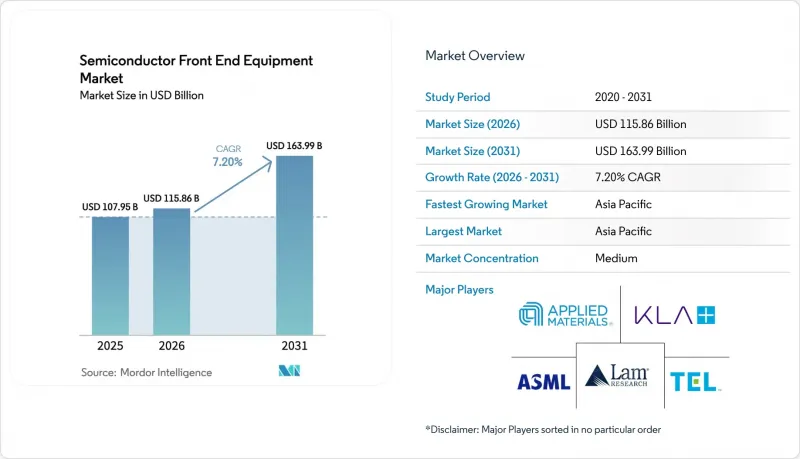
Mordor Intelligence에 의하면, 반도체 프론트엔드 장비 시장 규모는 2025년에 1,079억 5,000만 달러로 평가되었습니다. 2026년 1,158억 6,000만 달러에서 2031년까지 1,639억 9,000만 달러에 이를 것으로 예상되며, 예측 기간(2026-2031년) CAGR은 7.2%를 나타낼 전망입니다.
본 보고서는 장비 유형(리소그래피, 에칭, 증착 및 박막, 기타), 최종 사용자 산업(파운드리 및 로직, IDM, 메모리(DRAM 및 NAND), 특수 아날로그 및 파워),웨이퍼 크기(300mm, 200mm, 150mm 및 100mm), 공정 노드 기술(5nm 이하, 6-16nm, 28-65nm, 65nm 초과(성숙)), 그리고 지역별로 분류되어 있습니다. 시장 예측은 금액(달러) 기준으로 제시되어 있습니다.
세계의 반도체 프론트엔드 장비 시장 동향 및 인사이트
AI의 발전으로 가속화되는 3nm 미만 노드로의 전환
각 파운드리 기업들은 노드 전환 주기를 대폭 가속화하고 있으며, 기존 로드맵보다 수년 앞서 나노시트 공정을 양산에 도입하고 있습니다. 이러한 급속한 발전은 TSMC의 N2 공정 양산화, 인텔의 18A 라인,삼성의 2nm 게이트 올 어라운드(GAA) 공정 흐름에서 확인할 수 있으며, 이들 모두 선행하는 FinFET 공정에 비해 에칭 및 성막 공정이 약 30% 증가했습니다. 이러한 추가 공정으로 인해 생산 라인당 장비 수가 현저히 증가하고 있습니다. 게다가, 이러한 첨단 공정에 필수적인 EUV 스캐너를 공급할 수 있는 업체는 ASML뿐입니다. 그러나 ASML의 생산 능력에는 한계가 있어, 2026년공급 상한선은 약 90대로 예상되며, 이는 팹 가동 및 효과적인 생산 확대 능력에 중대한 제약을 가하고 있습니다.
HBM 주도 하의 TSV 및 심층 실리콘 에칭 수요 급증
각 메모리 제조업체들은 최대 12개의 다이를 적층하는 HBM3E 패키지의 발전에 힘입어, 심층 반응성 이온 에칭 장비와 구리 충전 증착 장비의 수주를 대폭 늘리고 있습니다. 이러한 적층 능력으로 인해 웨이퍼 1장당 수만 개에 달하는 높은 종횡비 비아가 필요하게 되어, 첨단 제조 장비의 사용이 필수적입니다. 램 리서치의 ‘Flex’ 플랫폼과 어플라이드 머티리얼즈의 ‘Sym3 Y’ 챔버는 모두 이 부문에서 두 자릿수의 대폭적인 수주 증가를 보고하고 있으며, 이는 메모리 생산 시장에서 이러한 기술에 대한 수요가 높아지고 있음을 여실히 보여주고 있습니다.
정밀 광학 부품 공급 병목 현상으로 인한 리드타임 장기화
세계의 모든 EUV 미러 세트는 칼 자이스 SMT에 의해 독점적으로 제조되고 있습니다. 이 회사의 오버코헨에 위치한 생산 시설은 표준 EUV 시스템용 연간 40세트, 고NA 툴용 연간 약 10세트를 생산할 수 있는 능력을 갖추고 있습니다. 이러한 제한된 생산 능력으로 인해 스캐너의 리드타임은 최대 30개월에 달할 수 있으며, 이는 공급망에 심각한 병목 현상을 초래하고 있습니다. 게다가 제조 공정에 어떤 차질이 발생하면 일정에 심각한 영향을 미쳐, 2nm 미만 기술의 양산 개시가 최대 18개월 지연될 가능성이 있습니다. ASML은 이러한 위험을 인식하고, 보다 견고하고 신뢰할 수 있는 공급망을 확보하기 위해 일본의 광학 기업과 제휴하여 듀얼 소싱 전략을 적극적으로 추진하고 있습니다.
부문별 분석
2025년에는 적극적인 파운드리 및 메모리 전략에 힘입어 리소그래피 장비가 매출의 28.94%를 차지했습니다. 이 장비들은 반도체 제조 공정에서 매우 중요한 역할을 수행하며, 첨단 칩 설계에 필요한 정밀한 패터닝을 가능하게 합니다. 대당 3억 8,000만 달러에 가까운 가격대의 고 NA EUV 플랫폼은 연평균 성장률(CAGR) 11.72%로 확대될 것으로 예상되며, 패터닝 기술과 관련된 반도체 프론트엔드 장비 시장을 주도할 전망입니다. 이러한 플랫폼에 대한 수요 증가는 반도체 소자의 복잡화에 대응하는 데 있어 그 중요성을 부각시키고 있습니다. 이에 이어 에칭 시스템이 22%의 점유율을 차지했습니다. 이는 게이트 올 어라운드(GaA) 구조의 중요성이 높아지고 있는 점과, 후면 전원 공급용 플라즈마 공정의 강화가 배경에 있습니다. 이러한 시스템은 현대 칩에 요구되는 복잡한 설계를 실현하는 데 필수적입니다. 박막 형성 장비는 19%의 점유율을 차지하며, 고유전율(high-k) 유전체에 대한 ALD(원자층 증착) 기술의 채택 확대를 뒷받침하고 있습니다. ALD의 보급 확대는 소자의 성능과 효율을 향상시키는 소재 및 공정으로의 산업적 전환을 반영하고 있습니다. 한편, 오버레이 관련 예산이 축소되었음에도 불구하고, 검사·계측 부문의 점유율은 12%로 상승했습니다. 이러한 성장은 반도체 제조에서 정밀한 품질 관리 및 측정에 대한 수요가 증가하고 있음을 보여줍니다.
이온 주입, CMP, 세정, 트랙 코트 현상액, 열처리 등 기존 카테고리는 지출의 나머지 18%를 차지했습니다. 이러한 카테고리는 성숙기에 접어들었음에도 불구하고, 반도체 제조 생태계 전체에 여전히 필수적입니다. 이러한 확고한 입지를 가진 공급업체들은 가격을 최대 25%까지 낮출 수 있는 급부상하는 중국 경쟁사들로부터 평균 판매 가격(ASP)에 대한 압박에 직면해 있습니다. 중국 경쟁사들의 가격 경쟁은 다국적 공급업체들에게 큰 과제가 되고 있습니다. 그 결과, 전 세계 공급업체들은 EUV, TSV, 액티닉 검사 등 수익성이 높은 제품 및 서비스로 연구개발(R&D) 투자를 전환하고 있습니다. 이러한 전략적 전환은 높은 이익률을 창출할 수 있는 기회를 활용하고, 끊임없이 변화하는 반도체 시장에서 경쟁 우위를 유지하기 위한 것입니다.
2025년에는 TSMC, 삼성 파운드리, 인텔이 파운드리 및 로직 제조업체를 주도하며 총 지출의 46.21%를 차지했습니다. 이들 기업은 첨단 제조 능력과 최첨단 기술에 대한 막대한 투자를 통해 꾸준히 시장을 선도해 왔습니다. 한편, SK하이닉스, 삼성, 마이크론이 주도하는 메모리 부문은 HBM 생산 능력 확대에 힘입어 연평균 성장률(CAGR) 10.40%라는 가장 빠른 성장이 예상됩니다. 메모리 부문의 이러한 급속한 성장은 기술 진보를 견인할 뿐만 아니라, 반도체 프론트엔드 장비 부문에서 TSV 에칭, 구리 충진, 웨이퍼 본딩 장비 시장 점유율 확대에도 기여하고 있습니다. 이러한 장비들은 고성능 메모리 솔루션의 생산을 가능하게 하는 데 필수적입니다.
텍사스 기기(Texas Instruments)와 인피니언(Infineon)이 자동차용 아날로그 및 파워 칩 제품 라인을 강화함에 따라, 통합 디바이스 제조업체는 지출의 18%를 차지하게 되었습니다. 이러한 변화는 특히 자동차가 첨단 전자 시스템에 대한 의존도를 높여감에 따라 반도체 산업에서 자동차 용도의 중요성이 커지고 있음을 여실히 보여줍니다. 한편, 전기차용 인버터 수요의 급증으로 특수 아날로그 및 파워 부문의 고객들이 힘을 얻어 나머지 12%를 차지했습니다. 이러한 수요는 반도체 시장 형성에서 전기차가 수행하는 역할이 확대되고 있음을 보여줍니다. 로직용에는 최첨단 리소그래피를, 메모리용에는 TSV와 박막 형성 기술을 우선시하는 등, 장비의 중점 부문에서 지속되는 분화가 공급업체의 전략에 계속해서 영향을 미치고 있습니다. 각 공급업체는 이러한 상이한 우선순위에 대응하기 위해 로드맵을 조정하며, 급속히 진화하는 시장 상황에서 경쟁력을 유지할 수 있도록 노력하고 있습니다.
지역별 분석
2025년, 아시아태평양은 55.17%라는 상당한 시장 점유율을 유지하며 그 우위를 지켰습니다. 이는 주로 대만의 첨단 반도체 허브, 한국의 대규모 메모리 생산 확대, 인도의 보조금 지원을 받은 팹의 적극적인 설립 덕분입니다. 대만만으로도 전 세계 반도체 제조 장비 수요의 약 25%를 차지하고 있으며, 대만의 N2, N2P, A16 생산 라인에서는 EUV 리소그래피 및 광측정 기술에 막대한 투자가 이루어졌습니다. 한편, 한국의 설비 투자는 HBM과 2nm 공정 추진에 중점을 두었으며, 생산 능력을 강화하기 위해 TSV, 유전체 에칭, 구리 충전 기술에 대한 대규모 수주가 집중되었습니다.
북미는 이에 이어 두 번째로 큰 기여 지역으로서, 세계 시장에서 22%의 매출 점유율을 확보했습니다. 이 지역의 성장에는 인텔의 오하이오주, 애리조나주, 오리건주 개발, 텍사스 기기의 300mm 아날로그 생산 라인 설립, 세계파운드리(GlobalFoundries)의 몰타 확장 계획과 같은 주요 프로젝트가 큰 영향을 미쳤습니다. 이러한 노력은 종합적으로 지역공급망을 재구축하고 있으며, 공급업체들은 이에 대응하여 현지 제조 거점 및 서비스 허브 설립을 추진하고 있습니다. 이러한 전략적 움직임은 ‘CHIPS 법’에 따라 제공되는 우대 조치를 활용하여 세계 반도체 시장에서 해당 지역의 위상을 더욱 강화하는 것을 목표로 하고 있습니다.
유럽은 약 12%의 시장 점유율을 차지하고 있으며, 그 초점은 특수 아날로그, 파워 반도체 부문, 고NA EUV 기술에 관한 선구적인 연구 이니셔티브에 집중되어 있었습니다. STMicroelectronics나 Infineon과 같은 기업들은 경쟁력을 유지하기 위해 비용 효율적인 성숙 노드 개발에 중점을 둔 반면, imec과 ASML의 협력으로 차세대 광 측정 솔루션이 추진되었습니다. 남미, 중동 및 아프리카는 여전히 세계 시장에서 기여도가 낮지만, 사우디아라비아가 지원하는 이니셔티브는 장기적인 성장 가능성을 시사하고 있습니다. 그러나 이러한 성장을 실현하기 위해서는 숙련된 인력 양성, 수자원 접근성 확보, 신뢰할 수 있는 공공 인프라 구축 등 생태계가 직면한 중요한 과제를 해결하는 것이 필수적입니다.
기타 혜택
- 엑셀 형식 시장 예측(ME) 시트
- 3개월간의 애널리스트 지원
자주 묻는 질문
목차
제1장 서론
제2장 조사 방법
제3장 주요 요약
제4장 시장 구도
제5장 시장 규모 및 성장 예측
제6장 경쟁 구도
제7장 시장 기회 및 향후 전망
KTH 26.09.14According to Mordor Intelligence, the semiconductor front-end equipment market size was valued at USD 107.95 billion in 2025 and estimated to grow from USD 115.86 billion in 2026 to reach USD 163.99 billion by 2031, at a CAGR of 7.2% during the forecast period (2026-2031).
This report is Segmented by Equipment Type (Lithography, Etch, Deposition and Thin-Film, and More), End-User Industry (Foundry and Logic, IDM, Memory DRAM and NAND, and Specialty Analog and Power), Wafer Size (300mm, 200mm, and 150mm and <=100mm), Process Node Technology (<=5nm, 6-16nm, 28-65nm, and >65nm Mature), and Geography. The Market Forecasts are Provided in Terms of Value (USD).
Global Semiconductor Front End Equipment Market Trends and Insights
AI-Accelerated Node Migration To Below 3 nm
Foundries are significantly accelerating their node-transition cycles, introducing nanosheet processes into production years ahead of their previously established roadmaps. This rapid advancement is evident in TSMC's N2 ramp, Intel's 18A line, and Samsung's 2 nm gate-all-around flow, all of which require approximately 30% more etch and deposition steps compared to their FinFET predecessors. These additional steps have led to a notable increase in the tool count per production line. Furthermore, only ASML has the capability to supply the essential EUV scanners required for these advanced layers. However, ASML's production capacity is limited, with a 2026 ceiling of approximately 90 units, which imposes significant constraints on fab start-ups and their ability to scale operations effectively.
HBM-Driven TSV And Deep-Silicon Etch Intensity Spike
Memory producers have significantly increased their orders for deep-reactive-ion etchers and copper-fill deposition tools, driven by the advancements in HBM3E packages, which now stack up to 12 dies. This stacking capability translates into tens of thousands of high-aspect-ratio vias per wafer, necessitating the use of advanced manufacturing tools. Both Lam Research's Flex platform and Applied Materials' Sym3 Y chamber have reported substantial double-digit order growth within this segment, highlighting the growing demand for these technologies in the memory production market.
Precision Optics Supply Bottlenecks Inflating Lead-Times
All EUV mirror sets globally are manufactured exclusively by Carl Zeiss SMT. The company's production facility in Oberkochen has the capacity to produce 40 assemblies annually for standard EUV systems and approximately 10 assemblies per year for High-NA tools. This limited production capacity results in scanner lead times that can extend up to 30 months, creating significant bottlenecks in the supply chain. Furthermore, any disruption in the production process could severely impact timelines, delaying the ramp-up of sub-2 nm technology by as much as 18 months. Recognizing these risks, ASML is actively pursuing dual sourcing strategies by collaborating with Japanese optics firms to ensure a more robust and reliable supply chain.
Other drivers and restraints analyzed in the detailed report include:
- Massive State-Backed Fab Build-Out In China
- High-NA EUV Roll-Out Spawning Actinic Metrology Demand
- Tightening Export Controls On Advanced Lithography
For complete list of drivers and restraints, kindly check the Table Of Contents.
Segment Analysis
In 2025, lithography tools accounted for 28.94% of the revenue, buoyed by assertive foundry and memory strategies. These tools play a critical role in the semiconductor manufacturing process, enabling precise patterning required for advanced chip designs. High-NA EUV platforms, each carrying a price tag close to USD 380 million, are set to expand at an 11.72% CAGR, propelling the semiconductor front-end equipment market tied to patterning technologies. The increasing demand for these platforms highlights their importance in meeting the growing complexity of semiconductor devices. Following closely, etch systems claimed a 22% share, driven by the rising prominence of gate-all-around structures and enhanced plasma steps for backside power delivery. These systems are essential for achieving the intricate designs required in modern chips. Deposition tools held a 19% stake, underscoring the growing adoption of ALD for high-k dielectrics. The wider use of ALD reflects the industry's shift towards materials and processes that enhance device performance and efficiency. Meanwhile, inspection and metrology climbed to a 12% share, even as overlay budgets tightened. This growth indicates the increasing need for precise quality control and measurement in semiconductor manufacturing.
Legacy categories, including ion implantation, CMP, cleaning, track-coat developers, and thermal processing, accounted for the remaining 18% of expenditures. These categories, while mature, remain vital to the overall semiconductor manufacturing ecosystem. Vendors entrenched in these established domains grapple with ASP pressures from swiftly advancing Chinese rivals, who can slash prices by as much as 25%. The competitive pricing from Chinese competitors poses significant challenges for multinational suppliers. As a result, global suppliers are redirecting R&D investments towards more lucrative offerings like EUV, TSV, and actinic inspection. This strategic shift aims to capitalize on higher-margin opportunities and maintain a competitive edge in the evolving semiconductor market.
In 2025, TSMC, Samsung Foundry, and Intel spearheaded the foundry and logic houses, accounting for 46.21% of the total expenditure. These companies have consistently led the market due to their advanced manufacturing capabilities and significant investments in cutting-edge technologies. Meanwhile, the memory segment, dominated by SK Hynix, Samsung, and Micron, is poised for the swiftest growth at a 10.40% CAGR, buoyed by HBM capacity expansions. This rapid growth in the memory sector is not only driving advancements in technology but also bolstering the market share of TSV etch, copper fill, and wafer-bonding tools in the semiconductor front-end equipment arena. These tools are critical for enabling the production of high-performance memory solutions.
Texas Instruments and Infineon, pivoting their lines for automotive analog and power chips, propelled integrated device manufacturers to capture 18% of the expenditures. This shift highlights the growing importance of automotive applications in the semiconductor industry, particularly as vehicles become increasingly reliant on advanced electronic systems. Meanwhile, a surge in demand for electric-vehicle inverters bolstered specialty analog and power customers, who claimed the remaining 12%. This demand underscores the expanding role of electric vehicles in shaping the semiconductor market. The ongoing divergence in equipment focus, prioritizing leading-edge lithography for logic and TSV and deposition for memory, continues to influence supplier strategies. Suppliers are adapting their roadmaps to address these distinct priorities, ensuring they remain competitive in a rapidly evolving market landscape.
Complete Report Scope:
- By Equipment Type
- Lithography Equipment
- Etch Equipment
- Deposition and Thin-Film Equipment
- Ion Implantation Equipment
- CMP Equipment
- Cleaning Equipment
- Inspection and Metrology
- Track, Coater and Developer
- Thermal Processing
- By End-User Industry
- Foundry and Logic
- IDM, Integrated Device Manufacturer
- Memory, DRAM and NAND
- Specialty Analog and Power
- By Wafer Size
- 300 mm
- 200 mm
- 150 mm and = 100 mm
- By Process Node Technology
- = 5 nm
- 6-16 nm
- 28-65 nm
- > 65 nm (Mature)
- By Geography
- North America
- United States
- Canada
- Mexico
- South America
- Brazil
- Argentina
- Rest of South America
- Europe
- Germany
- United Kingdom
- France
- Italy
- Spain
- Rest of Europe
- Asia Pacific
- China
- Japan
- South Korea
- India
- Australia
- New Zealand
- Rest of Asia-Pacific
- Middle East and Africa
- Middle East
- United Arab Emirates
- Saudi Arabia
- Turkey
- Rest of Middle East
- Africa
- South Africa
- Nigeria
- Kenya
- Rest of Africa
- Middle East
- North America
Geography Analysis
In 2025, the Asia-Pacific region maintained its dominance with a substantial 55.17% market share, primarily driven by Taiwan's advanced semiconductor hubs, South Korea's significant memory expansions, and India's proactive establishment of subsidy-supported fabs. Taiwan alone accounted for approximately 25% of the global demand for semiconductor tools, with its N2, N2P, and A16 production lines making substantial investments in EUV lithography and actinic metrology technologies. Meanwhile, South Korea's capital expenditures were heavily focused on advancing HBM and 2 nm processes, channeling significant orders toward TSV, dielectric etch, and copper fill technologies to enhance production capabilities.
North America followed as the second-largest contributor, securing a 22% revenue share in the global market. The region's growth was significantly influenced by major projects such as Intel's developments in Ohio, Arizona, and Oregon, Texas Instruments' establishment of 300 mm analog production lines, and GlobalFoundries' expansion efforts in Malta. These initiatives have collectively reshaped the regional supply chain, prompting equipment vendors to respond by setting up local manufacturing modules and service hubs. This strategic move aims to capitalize on the incentives provided under the CHIPS Act, further strengthening the region's position in the global semiconductor market.
Europe held an approximate 12% market share, with its focus centered on specialty analogs, power semiconductor sectors, and pioneering research initiatives for High-NA EUV technologies. Companies like STMicroelectronics and Infineon emphasized the development of cost-efficient mature nodes to remain competitive, while collaborations between imec and ASML advanced next-generation actinic metrology solutions. Although South America, the Middle East, and Africa remained minor contributors to the global market, initiatives backed by Saudi Arabia indicate potential long-term growth. However, realizing this growth will depend on addressing critical ecosystem challenges, including the development of skilled labor, access to water resources, and the availability of reliable utilities.
- Applied Materials Inc.
- KLA Corporation
- ASML Holding N.V.
- Lam Research Corporation
- Tokyo Electron Limited
- Nikon Corporation
- Canon Inc.
- SCREEN Holdings Co., Ltd.
- ASM International N.V.
- Advantest Corporation
- Disco Corporation
- Lasertec Corporation
- Axcelis Technologies Inc.
- Onto Innovation Inc.
- Veeco Instruments Inc.
- AMETEK Inc.
- Plasma-Therm LLC
- NAURA Technology Group Co., Ltd.
- Advanced Micro-Fab Equipment (AMEC) Inc.
- Shanghai Micro Electronics Equipment (SMEE) Co., Ltd.
- Ebara Corporation
- TEL Semes Co., Ltd.
- ULVAC Inc.
- ACCRETECH Inc. (Tokyo Seimitsu)
Additional Benefits:
- The market estimate (ME) sheet in Excel format
- 3 months of analyst support
TABLE OF CONTENTS
1 INTRODUCTION
- 1.1 Study Assumptions and Market Definition
- 1.2 Scope of the Study
2 RESEARCH METHODOLOGY
3 EXECUTIVE SUMMARY
4 MARKET LANDSCAPE
- 4.1 Market Overview
- 4.2 Market Drivers
- 4.2.1 AI-Accelerated Node Migration to Below 3 nm
- 4.2.2 Massive State-Backed Fab Build-Out in China
- 4.2.3 5G and IoT Device Rebound Lifting Mature-Node Demand
- 4.2.4 HBM-Driven TSV and Deep-Silicon Etch Intensity Spike
- 4.2.5 High-NA EUV Roll-Out Spawning Actinic Metrology Demand
- 4.2.6 India's Greenfield 300 mm Fabs (CHIPS-Linked) 2026-29
- 4.3 Market Restraints
- 4.3.1 Precision Optics Supply Bottlenecks Inflating Lead-Times
- 4.3.2 Tightening Export Controls on Advanced Lithography
- 4.3.3 Back-Side Power-Delivery Defect Hurdles Delaying Tools
- 4.3.4 Net-Zero Fab Mandates Raising Wet-Bench TCO
- 4.4 Industry Value-Chain Analysis
- 4.5 Regulatory Landscape
- 4.6 Technological Outlook
- 4.7 Porter's Five Forces Analysis
- 4.7.1 Bargaining Power of Buyers
- 4.7.2 Bargaining Power of Suppliers
- 4.7.3 Threat of New Entrants
- 4.7.4 Threat of Substitutes
- 4.7.5 Competitive Rivalry
5 MARKET SIZE AND GROWTH FORECASTS (VALUE)
- 5.1 By Equipment Type
- 5.1.1 Lithography Equipment
- 5.1.2 Etch Equipment
- 5.1.3 Deposition and Thin-Film Equipment
- 5.1.4 Ion Implantation Equipment
- 5.1.5 CMP Equipment
- 5.1.6 Cleaning Equipment
- 5.1.7 Inspection and Metrology
- 5.1.8 Track, Coater and Developer
- 5.1.9 Thermal Processing
- 5.2 By End-User Industry
- 5.2.1 Foundry and Logic
- 5.2.2 IDM, Integrated Device Manufacturer
- 5.2.3 Memory, DRAM and NAND
- 5.2.4 Specialty Analog and Power
- 5.3 By Wafer Size
- 5.3.1 300 mm
- 5.3.2 200 mm
- 5.3.3 150 mm and = 100 mm
- 5.4 By Process Node Technology
- 5.4.1 = 5 nm
- 5.4.2 6-16 nm
- 5.4.3 28-65 nm
- 5.4.4 > 65 nm (Mature)
- 5.5 By Geography
- 5.5.1 North America
- 5.5.1.1 United States
- 5.5.1.2 Canada
- 5.5.1.3 Mexico
- 5.5.2 South America
- 5.5.2.1 Brazil
- 5.5.2.2 Argentina
- 5.5.2.3 Rest of South America
- 5.5.3 Europe
- 5.5.3.1 Germany
- 5.5.3.2 United Kingdom
- 5.5.3.3 France
- 5.5.3.4 Italy
- 5.5.3.5 Spain
- 5.5.3.6 Rest of Europe
- 5.5.4 Asia Pacific
- 5.5.4.1 China
- 5.5.4.2 Japan
- 5.5.4.3 South Korea
- 5.5.4.4 India
- 5.5.4.5 Australia
- 5.5.4.6 New Zealand
- 5.5.4.7 Rest of Asia-Pacific
- 5.5.5 Middle East and Africa
- 5.5.5.1 Middle East
- 5.5.5.1.1 United Arab Emirates
- 5.5.5.1.2 Saudi Arabia
- 5.5.5.1.3 Turkey
- 5.5.5.1.4 Rest of Middle East
- 5.5.5.2 Africa
- 5.5.5.2.1 South Africa
- 5.5.5.2.2 Nigeria
- 5.5.5.2.3 Kenya
- 5.5.5.2.4 Rest of Africa
- 5.5.5.1 Middle East
- 5.5.1 North America
6 COMPETITIVE LANDSCAPE
- 6.1 Market Concentration
- 6.2 Strategic Moves
- 6.3 Market Share Analysis
- 6.4 Company Profiles (includes Global Level Overview, Market Level Overview, Core Segments, Financials as available, Strategic Information, Market Rank/Share, Products and Services, Recent Developments)
- 6.4.1 Applied Materials Inc.
- 6.4.2 KLA Corporation
- 6.4.3 ASML Holding N.V.
- 6.4.4 Lam Research Corporation
- 6.4.5 Tokyo Electron Limited
- 6.4.6 Nikon Corporation
- 6.4.7 Canon Inc.
- 6.4.8 SCREEN Holdings Co., Ltd.
- 6.4.9 ASM International N.V.
- 6.4.10 Advantest Corporation
- 6.4.11 Disco Corporation
- 6.4.12 Lasertec Corporation
- 6.4.13 Axcelis Technologies Inc.
- 6.4.14 Onto Innovation Inc.
- 6.4.15 Veeco Instruments Inc.
- 6.4.16 AMETEK Inc.
- 6.4.17 Plasma-Therm LLC
- 6.4.18 NAURA Technology Group Co., Ltd.
- 6.4.19 Advanced Micro-Fab Equipment (AMEC) Inc.
- 6.4.20 Shanghai Micro Electronics Equipment (SMEE) Co., Ltd.
- 6.4.21 Ebara Corporation
- 6.4.22 TEL Semes Co., Ltd.
- 6.4.23 ULVAC Inc.
- 6.4.24 ACCRETECH Inc. (Tokyo Seimitsu)
7 MARKET OPPORTUNITIES AND FUTURE OUTLOOK
- 7.1 White-Space and Unmet-Need Assessment


