

|
시장보고서
상품코드
2155328
반도체 웨이퍼 비전 검사 시스템 : 시장 점유율 분석, 업계 동향과 통계, 성장 예측(2026-2031년)Semiconductor Wafer Vision Inspection Systems - Market Share Analysis, Industry Trends & Statistics, Growth Forecasts (2026 - 2031) |
||||||
 Mordor Intelligence
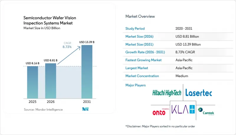
에 따르면 반도체 웨이퍼용 영상 검사 시스템 시장 규모는 2025년 81억 6,000만 달러, 2026년 88억 1,000만 달러에서 2031년까지 133억 9,000만 달러로 확대될 것으로 예측되고 있으며, 2026-2031년까지 연평균 성장률(CAGR)은 8.73%에 달할 전망입니다.
전 세계 반도체 웨이퍼 이미지 검사 시스템 시장의 동향 및 인사이트
AI를 활용한 결함 분류 및 폐쇄 루프 방식의 수율 관리
AI를 활용한 분류 기술을 통해 대량 생산되는 반도체 제조 과정에서 검사 결과와 수율 관리에 대한 의사결정이 보다 직접적으로 연계되고 있습니다. Onto Innovation사는 자사의 ‘ADC 토탈 솔루션’을 통해 300mm 리디스트리뷰션 층의 생산 테스트에서 1회 검사 실행당 노이즈 결함을 2,000건 이상에서 100건 미만으로 줄였다고 보고했습니다. 해당 보고서에 따르면 웨이퍼 수준의 패턴 분류 정확도가 100%를 달성했으며, 결함 누락률이 0.03% 미만인 것으로 나타났습니다. ASML은 자사의 ‘Computational Guided Inspection’이 Micron의 메모리 제조 기지에서 기존의 정적 샘플링 계획에 비해 불량 다이 검출률을 최대 4.3배 향상시켰다고 보고했습니다. 이러한 결과로 인해 수작업 검토의 부담이 경감되고, 공정 드리프트가 발생했을 때 팹이 보다 신속하게 대응할 수 있게 됩니다. 검사 플랫폼이 대량의 이미지를 생산 팀이 지체 없이 활용할 수 있는 판단으로 변환할 수 있다면, 반도체 웨이퍼 시각 검사 시스템 시장은 그 혜택을 누리게 될 것입니다.
첨단 노드 및 3D 디바이스의 복잡성
새로운 디바이스 아키텍처는 단순히 광학 감도의 향상을 요구할 뿐만 아니라, 수율을 제한할 수 있는 결함의 특성 자체를 변화시키고 있습니다. 게이트 올 어라운드(GAA) 디바이스의 경우, 기존의 고처리량 광학 기법으로는 식별하기 어려운 나노시트나 게이트 유전체 결함이 발생할 가능성이 있습니다. 애플라이드 매트리얼즈는 2025년 2월, 2nm 로직, 첨단 DRAM 및 3D NAND 제조 과정에서 매립된 나노 스케일 결함을 검출하기 위한 ‘SEMVision H20’ 시스템을 발표했습니다. KLA는 2025년 4월, 5nm 노드 이하의 고감도 로직 및 메모리 검사를 위해 3935 및 3920 EP 광대역 플라즈마 시스템을 발표했습니다. 설계 밀도가 향상됨에 따라 후공정 웨이퍼 처리 단계에서 결함이 확대되기 전에 필요한 검사 횟수도 증가하고 있습니다. 반도체 웨이퍼 시각 검사 시스템 시장은 제조사가 새로운 팹 생산 능력을 확충하지 않더라도 이러한 검사 빈도의 증가에 힘입어 성장하고 있습니다.
첨단 검사 장비에 대한 높은 설비 투자 및 통합 비용
첨단 광학 및 전자빔 플랫폼은 웨이퍼 팹 내에서 가장 고가의 개별 장비 구매 대상 중 하나입니다. 구매자가 높은 처리량, 더 높은 감도, 그리고 단일 플랫폼 상에서 여러 검사 기능을 필요로 할 경우 비용은 상승합니다. 하드웨어 구매는 투자의 일부에 불과합니다. 그 장비는 공정 제어 소프트웨어 및 자동 자재 이송 시스템과도 연동되어야 하기 때문입니다. AI를 활용한 워크플로는 고객에게 데이터 관리 및 모델 유지 관리에 대한 추가 요구 사항을 부과할 가능성이 있습니다. 소규모 제조사나 200mm 팹의 경우, 생산 경제성이 성숙한 노드를 기반으로 하므로 투자 회수 기간이 길어질 가능성이 있습니다. 이러한 상황으로 인해 최첨단 기술을 채택하지 않은 반도체 웨이퍼 시각 검사 시스템 시장의 일부에서는 장비 교체가 지연될 수 있습니다.
부문 분석
2025년, 광학 검사 시스템은 반도체 웨이퍼 시각 검사 시스템 시장 점유율의 68.23%를 차지했습니다. 명시야 및 암시야 플랫폼은 패터닝이 완료된 웨이퍼와 미패터닝 웨이퍼 워크플로우에서 높은 처리량을 실현하므로 여전히 널리 사용되고 있습니다. 또한 확립된 레시피 라이브러리를 통해 대량 생산을 수행하는 파운드리 및 메모리 공장에서 재현성이 높은 도입이 가능하며, 이는 반도체 웨이퍼 시각 검사 시스템 시장에서 실질적인 이점이 되고 있습니다. 고객은 각 생산 인증을 처음부터 시작하는 대신, 익숙한 워크플로우를 기반으로 구축할 수 있기 때문입니다. X선 검사 시스템은 첨단 패키징 및 실리콘 관통 비아(TSV) 웨이퍼 검사에서 증가하는 수요에 대응하고 있습니다. 가시광선 시스템으로는 도달 범위가 제한되는 깊은 곳까지 비파괴적인 이미징을 제공합니다.
전자빔 검사·리뷰 시스템은 2031년까지 연평균 성장률(CAGR) 10.60%로 확대될 것으로 예측됩니다. 이 시스템의 주요 강점은 광학 검사로는 감지하기 어려울 수 있는 매립층내 10nm 미만의 결함을 분해할 수 있다는 점에 있습니다. 게이트 올 어라운드(GaAA) 디바이스와 후면 전원 공급 네트워크의 보급으로 인해 접점 및 유전체 구조에 대한 전압 콘트라스트 검사의 가치가 높아지고 있습니다. KIOXIA 이와테는 2025년 9월, 포토일렉트론 서울과 나고야 대학이 공동 개발한 질화갈륨 기반 전자빔 플랫폼의 평가를 시작했습니다. 개발자들에 따르면 이 플랫폼은 기존 전자빔 광원에 비해 광음극의 내구성이 20배 이상 향상되어, 오랫동안 과제로 남아 있던 생산 처리량 제약을 해소하고 있습니다. 샘플 검사에서 인라인 사용으로의 전환에 따라 반도체 웨이퍼 시각 검사 시스템 시장의 장비 수요와 서비스 요구 사항이 증가할 가능성이 있습니다.
2025년, 패터닝된 웨이퍼 검사는 반도체 웨이퍼 시각 검사 시스템 시장의 73.14%를 차지하고 있으며, 2031년까지 연평균 성장률(CAGR) 11.30%로 확대될 것으로 예측됩니다. 이 범주는 공정층을 통해 웨이퍼 위에 디바이스 구조가 형성된 후에 사용됩니다. 다이 간 및 다이와 데이터베이스 간의 비교를 통해 공정상의 결함과 의도된 회로 레이아웃을 구별할 수 있습니다. 이는 피치가 좁아 결함 식별이 어려워지는 첨단 로직 및 메모리 노드에서 중요합니다. 패터닝 워크플로우내 반도체 웨이퍼 이미지 검사 시스템 시장의 규모는 후공정 전에 검사가 필요한 핵심 층의 수가 증가하고 있는 데 힘입어 성장하고 있으며, 이는 비용 증가로 이어지고 있습니다.
ASML은 2024년, 마이크론(Micron)의 DRAM 및 3D NAND 생산 기지에서 25개의 빔렛을 갖춘 다중 전자빔 시스템의 실증 시험을 시행했습니다. 이 플랫폼은 전압 콘트라스트 결함 감지를 주요 사용 사례로 삼고 있으며, 물리적 결함 감지는 부차적인 기능으로 자리매김하고 있습니다. 패터닝되지 않은 웨이퍼의 검사는 디바이스 제조 시작 전의 기판 입고 검사, 블랭킷 필름 모니터링 및 재료 특성 평가에 있으며, 여전히 필수적입니다. 이는 특히 실리콘 카바이드 및 갈륨 나이트라이드 웨이퍼에서 중요하며, 조기 선별을 통해 결함이 있는 재료의 추가 가공을 방지할 수 있습니다. 'Onto Innovation'지의 보고에 따르면 XY 스테이지를 이용한 광발광 스캐닝에서는 200mm 및 300mm 실리콘 카바이드 웨이퍼 전체에 걸쳐 중심에서 가장자리까지 일관된 감도가 유지되었습니다. 화합물 반도체 웨이퍼의 직경이 커짐에 따라 이 분야의 활용은 더욱 확대될 가능성이 있습니다.
지역별 분석
아시아태평양은 2025년 반도체 웨이퍼용 비전 검사 시스템 시장의 66.11%를 차지하고 있으며, 2031년까지 연평균 성장률(CAGR) 11.21%로 확대될 것으로 예측됩니다. 대만은 5nm 이하 노드에서 최첨단 파운드리 생산 능력이 집중되어 있으며, 웨이퍼당 높은 검사 밀도를 지원하고 있습니다. 한국에서는 HBM 및 첨단 DRAM으로의 전환이 맞물려 광학 및 전자빔 플랫폼에 대한 수요가 증가하고 있습니다. 중국은 국제 공급업체들이 수출 관련 규제에 직면한 반면, 국내 장비 제조사들이 생산 능력 확대를 도모하고 있으며, 다른 환경에 놓여 있습니다. 일본은 레이저테크(Lasertec)사와 그 ACTIS 제품군을 통해 EUV 마스크의 광선 검사 분야에서 독보적인 입지를 확립하고 있습니다.
북미 및 유럽에서는 신규 팹 건설과 국내 반도체 공급망에 대한 투자로 인해 장비 수요가 증가하고 있습니다. 미국의 인센티브 프로그램은 완전한 인증과 인라인 공정 제어 장비가 필요한 신규 시설을 지원하고 있습니다. ZEISS SMT는 첨단 노드 및 첨단 패키징 용도를 위한 반도체 검사, 계측, 결함 분석 솔루션에 대해 2026년 생산 능력 확대를 발표했습니다. 또한 유럽에는 반도체 웨이퍼 비전 검사 시스템 시장 전반을 지원하는 정밀 광학 기술의 기반이 마련되어 있습니다. 이러한 지역에서는 공급업체에게 현지 설치, 서비스 요구 사항 및 개별 생산 인증 관리를 요구하고 있습니다.
중동 및 아프리카 및 남미는 전 세계 웨이퍼 검사 수요에서 차지하는 비중이 비교적 작은 지역입니다. 이 지역에서의 활동은 최첨단 로직 팹보다는 특수 반도체, 조립, 테스트 및 기술 인프라와 관련이 있습니다. 아랍에미리트(UAE)와 사우디아라비아는 기술 인프라 구축을 추진하는 한편, 국내 테스트 및 패키징 역량에 관한 초기 단계의 협의를 진행하고 있습니다. 남미, 특히 브라질에서는 여전히 전자기기 제조 및 패키지된 부품 수요와의 연계가 더 강한 상황입니다. 이 지역들은 2031년까지 첨단 웨이퍼 검사 분야에서는 주변적인 위치를 유지할 것이지만, 향후 팹(제조 거점)의 다각화를 통해 반도체 웨이퍼 시각 검사 시스템 시장에 장기적인 기회가 창출될 가능성이 있습니다.
기타 혜택:
- 엑셀 형식의 시장 예측(ME) 시트
- 3개월간의 애널리스트 지원
자주 묻는 질문
목차
제1장 서론
- 조사 전제조건과 시장 정의
- 조사 범위
제2장 조사 방법
제3장 개요
제4장 시장 구도
- 시장 개요
- 거시경제 요인이 시장에 미치는 영향
- 시장 성장 촉진요인
- 시장 성장 억제요인
- 업계 밸류체인 분석
- 규제 상황
- 기술 전망
- Porter's Five Forces 분석
제5장 시장 규모와 성장 예측
- 시스템 유형별
- 웨이퍼 표면 및 패턴별
- 검사 모드별
- 용도별
- 최종사용자 산업별
- 지역별
- 북미
- 미국
- 캐나다
- 멕시코
- 남미
- 브라질
- 아르헨티나
- 기타 남미 국가
- 유럽
- 독일
- 영국
- 프랑스
- 이탈리아
- 스페인
- 기타 유럽 국가
- 아시아태평양
- 중국
- 일본
- 인도
- 한국
- ASEAN
- 기타 아시아태평양 국가
- 중동 및 아프리카
- 중동
- 사우디아라비아
- 아랍에미리트
- 튀르키예
- 기타 중동 국가
- 아프리카
- 남아프리카공화국
- 나이지리아
- 기타 아프리카 국가
- 중동
- 북미
제6장 경쟁 구도
- 시장 집중도
- 전략적 동향
- 시장 점유율 분석
- 기업 개요
- KLA Corporation
- Onto Innovation, Inc.
- Camtek Ltd.
- Lasertec Corporation
- Hitachi High-Tech Corporation
- Applied Materials, Inc.
- ASML Holding N.V.
- JEOL Ltd.
- Nikon Corporation
- Nova Ltd.
- Toray Engineering Co., Ltd.
- SCREEN Semiconductor Solutions Co., Ltd.
- Microtronic Inc.
- Confovis GmbH
- NEXTIN Co., Ltd.
- Muetec Co., Ltd.
- Nanotronics Imaging, Inc.
- Suzhou TZTEK Technology Co., Ltd.
- Wuhan Jingce Electronic Group Co., Ltd.
- Hangzhou Changchuan Technology Co., Ltd.
- Shanghai Micro Electronics Equipment(Group) Co., Ltd.
제7장 시장 기회와 향후 전망
KSA 26.10.28According to Mordor Intelligence, the semiconductor wafer vision inspection systems market size is projected to expand from USD 8.16 billion in 2025 and USD 8.81 billion in 2026 to USD 13.39 billion by 2031, registering a CAGR of 8.73% between 2026 to 2031.
Global Semiconductor Wafer Vision Inspection Systems Market Trends and Insights
AI-Enabled Defect Classification and Closed-Loop Yield Control
AI-based classification is linking inspection results more directly with yield-control decisions in high-volume semiconductor production. Onto Innovation reported that its ADC Total Solution reduced nuisance defects from more than 2,000 per inspection run to fewer than 100 in 300mm redistribution-layer production trials. The same work reported 100% wafer-level pattern classification accuracy and a defect escape rate below 0.03%. ASML reported that its Computational Guided Inspection improved defective-die capture by up to 4.3 times at Micron memory manufacturing sites when compared with static sampling plans. These results reduce the manual review burden and allow fabs to respond faster when a process drift appears. The semiconductor wafer vision inspection systems market benefits when inspection platforms can translate large volumes of images into decisions that production teams can use without delay.
Advanced-Node and 3D Device Complexity
New device architectures change the defects that can limit yield, rather than simply requiring finer optical sensitivity. Gate-all-around devices can introduce nanosheet and gate-dielectric defects that are difficult to identify through conventional high-throughput optical methods. Applied Materials introduced its SEMVision H20 system in February 2025 for buried nanoscale defects in 2nm logic, advanced DRAM, and 3D NAND production. KLA introduced its 3935 and 3920 EP broadband plasma systems in April 2025 for sensitive logic and memory inspection at 5nm nodes and below. Greater design density also increases the number of inspections needed before defects spread through later wafer-processing steps. The semiconductor wafer vision inspection systems market gains support from this higher inspection intensity, even when a manufacturer does not add new fab capacity.
High Capital and Integration Cost of Advanced Inspection Tools
Advanced optical and e-beam platforms are among the most expensive individual equipment purchases within a wafer fab. Costs rise when buyers require high throughput, greater sensitivity, and several inspection capabilities on one platform. The hardware purchase is only part of the commitment because the tool must also connect with process-control software and automated material-handling systems. AI-enabled workflows can add data management and model maintenance requirements for the customer. Smaller manufacturers and 200mm facilities can face a longer return period because their production economics are based on mature nodes. These conditions can slow equipment refreshes in parts of the semiconductor wafer vision inspection systems market that do not operate at the leading edge.
Other drivers and restraints analyzed in the detailed report include:
- Heterogeneous Integration, HBM, and Chiplet Packaging
- Fab Regionalization and Government-Supported Capacity Expansion
- Export Controls and Fragmented Compliance Requirements
For complete list of drivers and restraints, kindly check the Table Of Contents.
Segment Analysis
Optical inspection systems held 68.23% of the semiconductor wafer vision inspection systems market share in 2025. Bright-field and dark-field platforms remain widely used because they offer high throughput across patterned and unpatterned wafer workflows. Their established recipe libraries also support repeatable deployment at high-volume foundries and memory fabs, a practical advantage in the semiconductor wafer vision inspection systems market, as customers can build on familiar workflows rather than start each production qualification from scratch. X-Ray Inspection Systems serve a growing need in advanced packaging and through-silicon-via wafer inspection. They provide non-destructive subsurface imaging where visible-light systems have limited reach.
E-beam inspection and review systems are projected to expand at a 10.60% CAGR through 2031. Their main strength is the ability to resolve sub-10nm defects in buried layers that may not be visible through optical inspection. Gate-all-around devices and backside power delivery networks increase the value of voltage-contrast inspection for contacts and dielectric structures. KIOXIA Iwate began evaluating a gallium nitride-based e-beam platform in September 2025, jointly developed by Photoelectron Soul and Nagoya University. The developers reported more than 20 times greater photocathode durability than conventional e-beam sources, addressing a long-standing production throughput constraint. The move from sampled review toward inline use can increase tool demand and service requirements within the semiconductor wafer vision inspection systems market.
Patterned wafer inspection accounted for 73.14% of the semiconductor wafer vision inspection systems market in 2025 and is projected to expand at an 11.30% CAGR through 2031. The category is used after process layers have formed device features on the wafer. Die-to-die and die-to-database comparisons help separate process defects from the intended circuit layout. This is important at advanced logic and memory nodes, where tight pitches make defect identification more difficult. The semiconductor wafer vision inspection systems market size for patterned workflows is driven by the increasing number of critical layers that require inspection before subsequent processing, which adds cost.
ASML validated a 25-beamlet multi-electron-beam system at Micron DRAM and 3D NAND production sites in 2024. The platform identified voltage-contrast defects as its main use case and physical defects as a secondary capability. Unpatterned Wafer Inspection remains essential for incoming substrate qualification, blanket-film monitoring, and material characterization before device fabrication begins. It has particular relevance for silicon carbide and gallium nitride substrates, where early screening can prevent further processing of defective material. Onto Innovation reported that XY-stage photoluminescence scanning maintained center-to-edge sensitivity across 200mm and 300mm silicon carbide wafers. The category can gain further use as compound semiconductor wafer diameters grow.
Complete Report Scope:
- By System Type
- Optical Inspection Systems
- E-Beam Inspection and Review Systems
- X-Ray Inspection Systems
- Photoluminescence and Other Specialized Imaging Inspection Systems
- By Wafer Surface and Pattern
- Patterned Wafer Inspection
- Unpatterned Wafer Inspection
- By Inspection Mode
- Inline Inspection
- At-Line Inspection
- Offline and Laboratory Inspection
- By Application
- Defect Detection and Classification
- Pattern and Process Monitoring
- Wafer Qualification and Incoming Quality Control
- Critical Layer and Lithography Process Inspection
- Other Applications
- By End-User Industry
- Semiconductor Foundries
- Integrated Device Manufacturers
- Memory Manufacturers
- Outsourced Semiconductor Assembly and Test Companies
- Wafer Manufacturers and Specialty Substrate Producers
- By Geography
- North America
- United States
- Canada
- Mexico
- South America
- Brazil
- Argentina
- Rest of South America
- Europe
- Germany
- United Kingdom
- France
- Italy
- Spain
- Rest of Europe
- Asia-Pacific
- China
- Japan
- India
- South Korea
- ASEAN
- Rest of Asia-Pacific
- Middle East and Africa
- Middle East
- Saudi Arabia
- United Arab Emirates
- Turkey
- Rest of the Middle East
- Africa
- South Africa
- Nigeria
- Rest of Africa
- Middle East
- North America
Geography Analysis
Asia-Pacific held 66.11% of the semiconductor wafer vision inspection systems market in 2025 and is projected to expand at an 11.21% CAGR through 2031. Taiwan has dense leading-edge foundry capacity at sub-5nm nodes, which supports high inspection intensity per wafer. South Korea combines HBM and advanced DRAM transitions, increasing demand for optical and e-beam platforms. China presents a different environment because international suppliers face export-related restrictions while domestic equipment companies seek to expand their capabilities. Japan holds a distinct position in actinic EUV mask inspection through Lasertec and its ACTIS product family.
North America and Europe are gaining equipment demand from new fab construction and investments in domestic semiconductor supply chains. The U.S. incentive program supports new facilities that require full sets of qualifications and inline process-control equipment. ZEISS SMT announced a 2026 capacity expansion for semiconductor inspection, metrology, and defect-analysis solutions serving advanced-node and advanced-packaging applications. Europe also has a precision-optics base that supports the wider semiconductor wafer vision inspection systems market. These regions require suppliers to manage local installations, service needs, and separate production qualifications.
The Middle East and Africa and South America represent a smaller share of global wafer inspection demand. Their activity is linked more to specialty semiconductor, assembly, testing, and technology infrastructure than to leading-edge logic fabs. The United Arab Emirates and Saudi Arabia have pursued technology infrastructure and early discussions around domestic testing and packaging capacity. South America remains more closely tied to electronics manufacturing and packaged-component demand, especially in Brazil. These regions remain peripheral to advanced wafer inspection through 2031, but future fab diversification could create longer-term opportunities for the semiconductor wafer vision inspection systems market.
- KLA Corporation
- Onto Innovation, Inc.
- Camtek Ltd.
- Lasertec Corporation
- Hitachi High-Tech Corporation
- Applied Materials, Inc.
- ASML Holding N.V.
- JEOL Ltd.
- Nikon Corporation
- Nova Ltd.
- Toray Engineering Co., Ltd.
- SCREEN Semiconductor Solutions Co., Ltd.
- Microtronic Inc.
- Confovis GmbH
- NEXTIN Co., Ltd.
- Muetec Co., Ltd.
- Nanotronics Imaging, Inc.
- Suzhou TZTEK Technology Co., Ltd.
- Wuhan Jingce Electronic Group Co., Ltd.
- Hangzhou Changchuan Technology Co., Ltd.
- Shanghai Micro Electronics Equipment (Group) Co., Ltd.
Additional Benefits:
- The market estimate (ME) sheet in Excel format
- 3 months of analyst support
TABLE OF CONTENTS
1 INTRODUCTION
- 1.1 Study Assumptions and Market Definition
- 1.2 Scope of the Study
2 RESEARCH METHODOLOGY
3 EXECUTIVE SUMMARY
4 MARKET LANDSCAPE
- 4.1 Market Overview
- 4.2 Impact of Macroeconomic Factors on the Market
- 4.3 Market Drivers
- 4.3.1 AI-Enabled Defect Classification and Closed-Loop Yield Control
- 4.3.2 Advanced-Node and 3D Device Complexity
- 4.3.3 Heterogeneous Integration, HBM, and Chiplet Packaging
- 4.3.4 Automotive and Power Semiconductor Quality Requirements
- 4.3.5 Fab Regionalization and Government-Supported Capacity Expansion
- 4.3.6 Compound Semiconductor Adoption for EVs, 5G, and Power Electronics
- 4.4 Market Restraints
- 4.4.1 High Capital and Integration Cost of Advanced Inspection Tools
- 4.4.2 Shortage of Skilled Inspection and Process-Control Engineers
- 4.4.3 Export Controls and Fragmented Compliance Requirements
- 4.4.4 Optical and E-Beam Data-Volume and Compute Burden
- 4.5 Industry Value-Chain Analysis
- 4.6 Regulatory Landscape
- 4.7 Technological Outlook
- 4.8 Porter's Five Forces Analysis
- 4.8.1 Bargaining Power of Suppliers
- 4.8.2 Bargaining Power of Buyers
- 4.8.3 Threat of New Entrants
- 4.8.4 Threat of Substitutes
- 4.8.5 Intensity of Competitive Rivalry
5 MARKET SIZE AND GROWTH FORECASTS (VALUE)
- 5.1 By System Type
- 5.1.1 Optical Inspection Systems
- 5.1.2 E-Beam Inspection and Review Systems
- 5.1.3 X-Ray Inspection Systems
- 5.1.4 Photoluminescence and Other Specialized Imaging Inspection Systems
- 5.2 By Wafer Surface and Pattern
- 5.2.1 Patterned Wafer Inspection
- 5.2.2 Unpatterned Wafer Inspection
- 5.3 By Inspection Mode
- 5.3.1 Inline Inspection
- 5.3.2 At-Line Inspection
- 5.3.3 Offline and Laboratory Inspection
- 5.4 By Application
- 5.4.1 Defect Detection and Classification
- 5.4.2 Pattern and Process Monitoring
- 5.4.3 Wafer Qualification and Incoming Quality Control
- 5.4.4 Critical Layer and Lithography Process Inspection
- 5.4.5 Other Applications
- 5.5 By End-User Industry
- 5.5.1 Semiconductor Foundries
- 5.5.2 Integrated Device Manufacturers
- 5.5.3 Memory Manufacturers
- 5.5.4 Outsourced Semiconductor Assembly and Test Companies
- 5.5.5 Wafer Manufacturers and Specialty Substrate Producers
- 5.6 By Geography
- 5.6.1 North America
- 5.6.1.1 United States
- 5.6.1.2 Canada
- 5.6.1.3 Mexico
- 5.6.2 South America
- 5.6.2.1 Brazil
- 5.6.2.2 Argentina
- 5.6.2.3 Rest of South America
- 5.6.3 Europe
- 5.6.3.1 Germany
- 5.6.3.2 United Kingdom
- 5.6.3.3 France
- 5.6.3.4 Italy
- 5.6.3.5 Spain
- 5.6.3.6 Rest of Europe
- 5.6.4 Asia-Pacific
- 5.6.4.1 China
- 5.6.4.2 Japan
- 5.6.4.3 India
- 5.6.4.4 South Korea
- 5.6.4.5 ASEAN
- 5.6.4.6 Rest of Asia-Pacific
- 5.6.5 Middle East and Africa
- 5.6.5.1 Middle East
- 5.6.5.1.1 Saudi Arabia
- 5.6.5.1.2 United Arab Emirates
- 5.6.5.1.3 Turkey
- 5.6.5.1.4 Rest of the Middle East
- 5.6.5.2 Africa
- 5.6.5.2.1 South Africa
- 5.6.5.2.2 Nigeria
- 5.6.5.2.3 Rest of Africa
- 5.6.5.1 Middle East
- 5.6.1 North America
6 COMPETITIVE LANDSCAPE
- 6.1 Market Concentration
- 6.2 Strategic Moves
- 6.3 Market Share Analysis
- 6.4 Company Profiles (includes Global Level Overview, Market Level Overview, Core Segments, Financials as available, Strategic Information, Market Rank/Share, Products and Services, Recent Developments)
- 6.4.1 KLA Corporation
- 6.4.2 Onto Innovation, Inc.
- 6.4.3 Camtek Ltd.
- 6.4.4 Lasertec Corporation
- 6.4.5 Hitachi High-Tech Corporation
- 6.4.6 Applied Materials, Inc.
- 6.4.7 ASML Holding N.V.
- 6.4.8 JEOL Ltd.
- 6.4.9 Nikon Corporation
- 6.4.10 Nova Ltd.
- 6.4.11 Toray Engineering Co., Ltd.
- 6.4.12 SCREEN Semiconductor Solutions Co., Ltd.
- 6.4.13 Microtronic Inc.
- 6.4.14 Confovis GmbH
- 6.4.15 NEXTIN Co., Ltd.
- 6.4.16 Muetec Co., Ltd.
- 6.4.17 Nanotronics Imaging, Inc.
- 6.4.18 Suzhou TZTEK Technology Co., Ltd.
- 6.4.19 Wuhan Jingce Electronic Group Co., Ltd.
- 6.4.20 Hangzhou Changchuan Technology Co., Ltd.
- 6.4.21 Shanghai Micro Electronics Equipment (Group) Co., Ltd.
7 MARKET OPPORTUNITIES AND FUTURE OUTLOOK
- 7.1 White-Space and Unmet-Need Assessment

(주말 및 공휴일 제외)


