

|
시장보고서
상품코드
2117510
3D 적층 DRAM 시장 : 점유율 분석, 업계 동향과 통계, 성장 예측(2026-2031년)3D-Stacked DRAM - Market Share Analysis, Industry Trends & Statistics, Growth Forecasts (2026 - 2031) |
||||||
 Mordor Intelligence
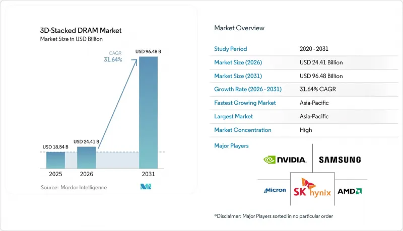
Mordor Intelligence에 의하면, 3D 적층 DRAM 시장 규모는 2025년 185억 4,000만 달러에서 2026년에는 244억 1,000만 달러로 확대되어 2026년부터 2031년까지 CAGR 31.6%로 성장을 지속하여, 2031년에는 964억 8,000만 달러에 이를 것으로 예측됩니다.
본 보고서는 아키텍처(하이브리드 메모리 큐브 및 유사 아키텍처, 기타), 스택당 메모리 용량(4GB, 8GB, 기타),프로세서 인터페이스(GPU, AI 가속기/ASIC, 기타), 용도(AI 및 데이터센터 서버, 고성능 컴퓨팅, 기타), 지역(북미, 유럽, 아시아태평양, 기타)별로 분류되어 있습니다. 예측치는 금액(미 달러)으로 표시되어 있습니다.
전 세계 3D 적층 DRAM 시장 동향 및 인사이트
AI 서버 및 가속기의 보급 확대
3D 적층 DRAM 시장은 단순히 서버 출하 대수가 증가한 것뿐만 아니라, 대규모 모델 학습 및 추론으로 인해 시스템당 메모리 수요가 증가함에 따라 그 양상이 급변하고 있습니다. 현재 AI 가속기에는 매우 높은 로컬 메모리 대역폭이 요구되고 있으며, 이로 인해 적층 메모리는 단순한 부수적인 부품이 아닌 시스템 설계의 핵심 요소가 되고 있습니다. NVIDIA는 2026년 1월, 자사의 Rubin 플랫폼이 GPU당 288GB의 HBM4를 통합하여 22TB/s의 대역폭을 실현했다고 밝혔습니다. 이에 따라 이전 세대에 비해 가속기 패키지당 메모리 탑재량이 대폭 증가했습니다. 또한 삼성도 2026년 2월에 HBM4 출하를 시작하며, 이 전환을 상용 공급 단계로 진전시켰습니다. 이는 제품 주기의 다음 단계가 더 이상 이론상의 이야기가 아니라, 이미 본격적인 도입 단계에 접어들었음을 보여줍니다. 이러한 변화에 따라 제조업체의 인센티브도 변화합니다. 왜냐하면 최첨단 웨이퍼 생산 능력은 기존 DRAM보다 HBM에서 훨씬 더 높은 가치를 창출할 수 있기 때문에 주요 공급업체에게는 적층형 제품을 계속 우선시할 명확한 이유가 있기 때문입니다. 그 결과, 메모리 시장 전체의 일부가 침체기를 맞이하더라도 3D 적층 DRAM 시장은 엄격한 생산 능력 배분을 통해 계속해서 지지를 받을 가능성이 높습니다.
추론 클러스터로의 HBM 전환
3D 적층 DRAM 시장은 워크로드 구성의 변화로도 혜택을 받고 있습니다. 이는 컨텍스트 윈도우, 사용자의 동시 실행 수, 모델의 복잡성이 증가함에 따라 추론 클러스터에는 더 대규모의 상주 메모리 풀이 필요하기 때문입니다. 이로 인해 출하되는 메모리 스택의 수가 증가할 뿐만 아니라, 각 스택의 권장 용량도 상승하여 고밀도 구성의 상업적 매력이 높아집니다. JEDEC의 HBM4 규격은 2,048비트 인터페이스, 32개의 독립 채널, 그리고 큐브당 최대 64GB 지원을 규정함으로써 이러한 전환을 뒷받침했습니다. 이를 통해 시스템 설계자는 컨트롤러를 완전히 재설정하지 않고도 대용량으로의 확장을 위한 명확한 로드맵을 확보할 수 있습니다. Samsung Electronics가 2026년 2월에 업데이트한 로드맵에는 2027년에 맞춤형 HBM 샘플이 고객에게 제공될 것이라고 명시되어 있으며, 이는 하이퍼스케일러 및 가속기 벤더들이 추론 요구 사항에 맞추어 메모리 설계를 보다 직접적으로 형성하는 조달 모델을 시사합니다. 이는 중요한 점입니다. 왜냐하면 3D 적층 DRAM 시장은 더 이상 범용 GPU의 수명 주기에만 얽매이지 않고, 워크로드의 특성에 밀접하게 부합하는 메모리를 요구하는 더 폭넓은 구매자층에 의해 지탱되고 있기 때문입니다. 그 결과, 특히 북미에서 추론 인프라의 확충이 대용량 HBM의 잠재 고객 기반을 확대하고 있어 수요의 하한선이 더욱 안정적으로 자리 잡고 있습니다.
TSV 및 패키징 수율이 걸림돌
3D 적층 DRAM 시장은 여전히 근본적인 제조상의 과제에 직면해 있습니다. 이는 수직 적층이 기존의 평면형 DRAM보다 더 높은 수준의 결함 위험을 초래하기 때문입니다. 실리콘 관통 비아(TSV)는 미세하고 깊으며, 그 수가 많기 때문에 제조 및 후속 조립 공정에서 보이드, 심 결함, 구리 충전 불균형이 발생하기 쉽습니다. SemiEngineering사는 TSV의 복잡성이 여전히 제조상의 병목 현상으로 작용하고 있다고 지적하고 있으며, 이는 사용자가 제공한 자료 전반에 걸쳐 언급된 지속적인 수율 저하와도 일치합니다. 공급업체들이 12층 고밀도 HBM4 스택으로 전환함에 따라 이 문제는 더욱 심각해질 것입니다. 층 수가 늘어날수록 웨이퍼의 얇은 절삭, 스택의 정렬, 그리고 본딩의 정합성에 대한 허용 오차가 줄어들기 때문입니다. 수요가 견조하더라도 백엔드 공정에서의 손실이 여전히 높은 수준을 유지한다면, 실질적인 생산량은 선형적으로 증가하지 않습니다. 따라서 3D 적층 DRAM 시장은 최종 시장 수요만으로 추측되는 것보다 공급 측면의 제약이 더 강해지고 있습니다. 이는 프리미엄 가격 책정이 지속되고 있는 이유 중 하나이기도 합니다. 왜냐하면 낮은 수율로 생산하면 고객에게 전달되는 인증된 제품 1개당 비용의 하한선을 사실상 끌어올리기 때문입니다.
부문 분석
2025년, HBM은 3D 적층 DRAM 시장 점유율의 73.6%를 차지하고 있으며, 이는 AI 가속기 수요가 얼마나 고대역폭·저지연 적층 제품에 집중되어 있는지를 여실히 보여줍니다. 3D 적층 DRAM 시장에서 이러한 위상은 일시적인 가격 효과라기보다는 설계상의 현실을 반영한 것입니다. 최첨단 AI 칩에는 로직 회로 근처에 배치할 수 있고, 비트당 전력 소비를 억제하면서도 매우 대용량의 데이터를 전송할 수 있는 메모리가 필요하기 때문입니다. 현재 이 아키텍처는 주요 가속기 프로그램에서의 HBM3E 및 HBM4 도입 주기를 통해 정착되었으며, 이를 통해 HBM은 기존 적층 방식에 대한 우위를 더욱 확대했습니다. JEDEC의 HBM4 규격은 HBM3 컨트롤러와의 하위 호환성을 유지하면서 다음 성능 기준을 정의함으로써 이러한 방향성을 더욱 공고히 했습니다. 이를 통해 시스템 설계자의 전환 작업 부담이 줄어듭니다. 3D 적층 DRAM 업계에서 HBM은 더 이상 수많은 선택지 중 하나가 아니라, 프리미엄 가속기 메모리의 기준이 되는 아키텍처로 자리 잡았습니다.
다른 아키텍처도 여전히 중요하지만, 그 이용 사례는 더 제한적입니다. 3DS DDR 및 TSV 적층형 기존 DRAM 부문은 대역폭 요구 사항이 낮고, 피크 밀도보다 인증된 안정성이 중시되는 고신뢰성 및 서버 버퍼 메모리 용도를 위해 계속해서 제공되고 있습니다. 하이브리드 메모리 큐브(HMC) 및 관련 설계는 특정 네트워크 및 통신 용도에서 여전히 채택되고 있으며, 그 밖의 적층형 변형들은 엣지 AI 및 모바일 관련 워크로드를 지원하고 있습니다. 가장 빠르게 성장하는 하위 부문은 ‘신흥 하이브리드 본딩 및 모놀리식 3D DRAM’으로, 3D 적층 DRAM 시장이 기존의 열압축 본딩의 범위를 넘어 발전함에 따라 2031년까지 연평균 성장률(CAGR) 34.4%로 확대될 것으로 예측됩니다. 삼성의 2026년 HBM4 출시와 SK하이닉스의 HBM4개발 로드맵은 모두 패키징 및 본딩 기법이 단순한 제조상의 세부 사항이 아니라 아키텍처 선택의 일부가 된다는 더 광범위한 변화를 시사합니다. 그 결과, 3D 적층 DRAM 시장의 아키텍처 구성 비율은 상위 계층에서는 안정적이지만, 하위 계층에서는 보다 역동적인 움직임이 나타나고 있으며, 본딩 기술이 다음 차별화의 물결을 형성하고 있습니다.
2025년 3D 적층 DRAM 시장 규모에서 16GB 구성은 33.8%의 점유율을 차지했습니다. 이는 지난 가속기 사이클에서 주류를 이루었던 HBM3E 8-high 제품에 의해 형성된 도입 기반을 반영한 것입니다. 실용적인 관점에서 볼 때, 16GB 적층 제품은 이미 양산되고 있는 대규모 AI 배포 환경에서 대역폭, 열 특성, 패키지 복잡성 간의 균형이 잘 잡혀 있어 양산량의 최적점이 되었습니다. 저밀도의 4GB 및 8GB 포맷은 메모리 실적가 최신 AI 가속기와 동등한 규모에 아직 도달하지 않은 기존 HPC, 네트워크용 ASIC 및 FPGA 용도에서 여전히 활용되고 있습니다. 한편, HBM4의 상용화가 진행됨에 따라 24GB 구성이 부상하고 있으며, 삼성은 12층 스택을 채택한 24GB 및 36GB 버전의 첫 상용 HBM4를 출하했다고 발표했습니다. 또한, JEDEC의 HBM4 규격은 16층 스택으로 큐브당 최대 64GB를 지원함으로써 단기적인 고밀도화의 길을 열었습니다. 이를 통해 수년에 걸친 가속기 플랫폼을 계획하고 있는 고객들에게 용량 확장 로드맵이 더욱 명확해졌습니다.
32GB 이상 부문은 2031년까지 32.7%라는 가장 높은 연평균 성장률(CAGR)을 보일 것으로 예상되며, 이러한 성장 속도는 새로운 가속기 세대가 등장할 때마다 패키지당 최소 메모리 요구 사항이 높아지는 추세와 일치합니다. NVIDIA에 따르면, Rubin R100 GPU는 288GB의 HBM4를 통합하여 22TB/s의 대역폭을 실현하고 있으며, 이는 단순히 스택 수를 늘리는 것이 아니라 더 고밀도인 스택 구성으로의 명확한 전환을 시사합니다. 3D 적층 DRAM 시장에서 이러한 변화는 중요한 의미를 지닙니다. 인터포저의 면적이나 조립 슬롯이 실리콘 비용과 마찬가지로 제약 요인으로 작용하기 때문에 소형 스택을 다수 마련하는 것보다 스택 수를 줄여 고밀도를 추구하는 것이 상업적으로 더 타당한 경우가 많기 때문입니다. 따라서 3D 적층 DRAM 업계는 특히 랙 스케일 시스템으로 인해 총 메모리 수요가 대폭 증가하고 있는 상황을 감안하여, 양에서 밀도로 논의의 초점이 옮겨가고 있습니다. 삼성의 24GB 및 36GB 출시 시점과 JEDEC의 64GB 상한선은 용량 로드맵이 이미 이러한 변화에 부합하고 있음을 보여줍니다. 그 결과, 3D 적층 DRAM 시장에서는 예측 기간 동안 수요의 중심이 용량 곡선의 상단으로 이동할 것으로 보입니다.
지역별 분석
아시아태평양은 2025년에 3D 적층 DRAM 시장 규모의 66.7%를 차지하며, 2031년까지 연평균 성장률(CAGR) 32.4%로 확대될 것으로 예측됩니다. 이 지역이 3D 적층 DRAM 시장의 기반을 이루고 있는 이유는 한국에 주요 HBM 제조업체들이 거점을 두고 있으며, 대만이 첨단 코패키징 및 인터포저 기술의 중심지로 자리 잡고 있기 때문입니다. 삼성이 2026년 2월에 상용 HBM4를 출시하고, SK하이닉스가 2025년 9월에 HBM4개발 마일스톤을 달성한 것은 시장의 기술적 방향성이 여전히 한국 공급업체에 크게 좌우되고 있음을 여실히 보여줍니다. 이러한 지역적 집중은 규모와 실행 면에서 우위를 가져다주지만, 한편으로는 일부 거점의 생산 능력 부족이나 패키징 지연이 3D 적층 DRAM 시장 전체에 영향을 미칠 가능성도 있음을 의미합니다. 일본은 반도체 공급의 회복탄력성 향상을 목표로 한 새로운 HBM 관련 투자 활동과 정책 지원을 통해 아시아태평양의 기반을 강화하고 있으며, 이로 인해 해당 지역은 현재 한국과 대만을 중심으로 한 틀을 넘어 확장되고 있습니다.
북미의 3D 적층 DRAM 시장은 해당 지역이 여전히 AI 가속기 시스템의 최대 구매처이기 때문에 생산 규모보다는 최종 수요에 의해 주도되고 있습니다. 클라우드 및 하이퍼스케일러의 견조한 주문 덕분에, 공급의 상당 부분이 아시아태평양에서 제조 및 패키징되더라도 북미는 3D 적층 DRAM 시장의 주요 상업적 견인력이 되고 있습니다. NVIDIA의 Rubin 플랫폼 출시는 이러한 수요 견인의 직접적인 사례입니다. 미국에 기반을 둔 가속기 공급업체의 플랫폼 변경은 전 세계 공급망 전반에 걸쳐 새로운 메모리 요구 사항으로 신속하게 반영되기 때문입니다. 또한, 미국의 산업 정책도 중요한 요소입니다. 국내 반도체 산업의 확대와 수출 관리 체계가 첨단 메모리 시스템의 제조, 판매, 도입이 가능한 장소를 결정하기 때문입니다. 유럽은 여전히 2차적인 수요 거점이지만, 각국 정부 주도의 AI 클라우드 프로그램 및 HPC(고성능 컴퓨팅) 도입에 힘입어 3D 적층 DRAM 시장에서 이 지역의 역할은 꾸준히 공고해지고 있습니다.
세계 기타 지역은 3D 적층 DRAM 시장에서 여전히 규모는 작지만, 새로운 데이터센터와 국가 주도의 AI 프로그램으로 인해 향후 수요 범위가 확대되고 있습니다. 중국은 현재의 수출 규제 하에서도 시장에 여전히 중요한 존재입니다. 왜냐하면 현행 세대의 HBM에 대한 접근이 라이선싱 규정에 의해 제한되는 반면, 구세대 기술을 활용한 국내 DRAM 생산 확대는 지속될 수 있기 때문입니다. 이로 인해 3D 적층 DRAM 시장의 최첨단 기술은 중국 외부에 집중된 채로 남아 있는 반면, 중국 공급업체들은 최첨단 기술 이하의 영역에서 국내 역량 강화에 주력하는 이중적인 구조가 형성되고 있습니다. 앞으로 이 시장의 지역은 이론상 수요가 존재하는 곳이라기보다는 제조, 첨단 패키징, 수출 규정 준수, 그리고 최종 시스템 도입이 모두 조화를 이룰 수 있는 곳에 의해 정의될 것입니다.
기타 혜택:
- 엑셀 형식 시장 예측(ME) 시트
- 3개월간의 애널리스트 지원
자주 묻는 질문
목차
제1장 서론
제2장 조사 방법
제3장 개요
제4장 시장 구도
제5장 시장 규모와 성장 예측
제6장 경쟁 구도
제7장 시장 기회와 향후 전망
JHS 26.09.01According to Mordor Intelligence, the 3D-Stacked DRAM market size is expected to grow from USD 18.54 billion in 2025 to USD 24.41 billion in 2026 and is forecast to reach USD 96.48 billion by 2031 at 31.6% CAGR over 2026-2031.
This report is Segmented by Architecture (Hybrid Memory Cube and Similar Architectures, and More), Memory Capacity Per Stack (4 GB, 8 GB, and More), Processor Interface (GPU, AI Accelerator/ASIC, and More), Application (AI and Data Center Servers, High-Performance Computing, and More), and Geography (North America, Europe, Asia-Pacific, and More). The Forecasts are Provided in Terms of Value (USD).
Global 3D-Stacked DRAM Market Trends and Insights
AI Server And Accelerator Ramp
The 3D-Stacked DRAM market is being reshaped by the way large-scale model training and inference have raised memory demand per system rather than simply increasing the number of servers shipped. AI accelerators now require very high local memory bandwidth, which makes stacked memory central to system design instead of a secondary bill-of-materials item. NVIDIA disclosed in January 2026 that its Rubin platform integrated 288 GB of HBM4 per GPU and delivered 22 TB/s of bandwidth, which materially lifted memory content per accelerator package compared with the prior generation. Samsung also moved this transition into commercial supply in February 2026 by beginning HBM4 shipments, showing that the next step in the product cycle is no longer theoretical and is already entering active deployment. That shift changes producer incentives because advanced wafer capacity can earn far more value in HBM than in conventional DRAM, so leading suppliers have a clear reason to keep prioritizing stacked products. As a result, the 3D-Stacked DRAM market is likely to remain supported by disciplined capacity allocation even when parts of the broader memory market move through slower phases.
HBM Migration To Inference Clusters
The 3D-Stacked DRAM market is also gaining from a change in workload mix, because inference clusters need larger resident memory pools as context windows, user concurrency, and model complexity rise. This not only increases the number of memory stacks shipped, but it also raises the preferred capacity of each stack and makes denser configurations more commercially attractive. JEDEC's HBM4 standard strengthened that transition by setting a 2,048-bit interface, 32 independent channels, and support for up to 64 GB per cube, which gives system designers a clear path to higher-capacity deployment without a full controller reset. Samsung's February 2026 roadmap update also showed that custom HBM samples will reach customers in 2027, which points to a procurement model where hyperscalers and accelerator vendors shape memory design more directly around inference needs. That matters because the 3D-Stacked DRAM market is no longer tied only to merchant GPU cycles and is increasingly supported by a wider buyer set that wants memory closely matched to workload behavior. The result is a steadier demand floor, especially in North America, where inference buildouts are broadening the addressable base for high-capacity HBM.
TSV And Packaging Yield Drag
The 3D-Stacked DRAM market still faces a fundamental manufacturing challenge because vertical stacking introduces defect risk to a greater degree than conventional planar DRAM. Through-silicon vias are small, deep, and numerous, making them vulnerable to voids, seam defects, and copper-fill variation during fabrication and later assembly. SemiEngineering noted that TSV complexity remains a manufacturing bottleneck, which aligns with the persistent yield drag described across the user-supplied material. The problem becomes harder as suppliers move to 12-high, denser HBM4 stacks, because wafer thinning, stack alignment, and bond integrity become less forgiving at higher layer counts. Even when demand is strong, usable output does not scale linearly if backend losses remain elevated, which keeps the 3D-Stacked DRAM market more supply-constrained than end-market demand alone would imply. This is one reason premium pricing has remained durable, since low-yield production effectively raises the cost floor for every qualified unit that reaches customers.
Other drivers and restraints analyzed in the detailed report include:
- HBM4 And Higher-Stack Transition
- Advanced Packaging And Hybrid Bonding Gains
- CoWoS And Backend Capacity Bottlenecks
For complete list of drivers and restraints, kindly check the Table Of Contents.
Segment Analysis
HBM held 73.6% of the 3D-Stacked DRAM market share in 2025, underscoring how firmly AI accelerator demand has centered on high-bandwidth, low-latency stacks. In the 3D-Stacked DRAM market, this position reflects a design reality rather than a temporary pricing effect, because leading AI chips need memory that can sit close to logic and move very large data volumes with lower power per bit. The architecture is now anchored by HBM3E and HBM4 deployment cycles across leading accelerator programs, and that has widened HBM's lead over older stacked approaches. JEDEC's HBM4 standard reinforced this direction by defining the next performance baseline while preserving backward compatibility with HBM3 controllers, which shortens transition work for system designers. Within the 3D-Stacked DRAM industry, that makes HBM is the reference architecture for premium accelerator memory rather than one option among several.
Other architectures still matter, but they operate in narrower use cases. The 3DS DDR and TSV-stacked conventional DRAM segment continues to serve high-reliability and server-buffered memory applications where bandwidth needs are lower, and qualification stability matters more than peak density. Hybrid Memory Cube and related designs remain present in selected networking and telecommunications roles, while other stacked variants support edge AI and mobile-adjacent workloads. The fastest-growing sub-segment is Emerging Hybrid-Bonded and Monolithic 3D DRAM, which is projected to expand at a 34.4% CAGR through 2031 as the 3D-Stacked DRAM market moves beyond conventional thermal compression bonding. Samsung's 2026 HBM4 launch and SK hynix's HBM4 development path both point toward a broader shift where packaging and bonding methods become part of architectural choice, not just manufacturing detail. That leaves the architecture mix in the 3D-Stacked DRAM market stable at the top but more dynamic beneath the surface, where bonding technology is setting up the next round of differentiation.
The 16 GB configuration accounted for 33.8% share of the 3D-Stacked DRAM market size in 2025, reflecting the installed base created by dominant HBM3E 8-high products in the prior accelerator cycle. In practical terms, 16 GB stacks were the volume sweet spot because they balanced bandwidth, thermals, and package complexity for large AI deployments already in production. Lower-density 4 GB and 8 GB formats still served legacy HPC, networking ASIC, and FPGA uses where memory footprints had not yet moved to the same scale as modern AI accelerators. At the same time, 24 GB configurations are gaining ground as HBM4 enters commercialization, and Samsung stated that its first commercial HBM4 shipped in both 24 GB and 36 GB versions using 12-layer stacks. JEDEC's HBM4 standard also opened a path toward higher near-term density by supporting up to 64 GB per cube in 16-high stacks, which makes the capacity ladder clearer for customers planning multi-year accelerator platforms.
The 32 GB and Above segment is projected to record the fastest 32.7% CAGR through 2031, and that pace fits the way each new accelerator generation is lifting the minimum memory requirement per package. NVIDIA said the Rubin R100 GPU integrates 288 GB of HBM4 with 22 TB/s bandwidth, which implies a clear move toward denser stack configurations rather than simple growth in stack count alone. In the 3D-Stacked DRAM market, that change is important because interposer area and assembly slots are now just as limiting as silicon cost, so fewer and denser stacks often make more commercial sense than a larger number of smaller ones. The 3D-Stacked DRAM industry is therefore shifting from a volume discussion to a density discussion, especially as rack-scale systems push total memory needs much higher. Samsung's 24 GB and 36 GB launch points, together with JEDEC's 64 GB ceiling, show that the capacity roadmap is already aligned with this shift. As a result, the 3D-Stacked DRAM market is likely to see the center of demand move upward on the capacity curve through the forecast period.
Complete Report Scope:
- By 3D-Stacked DRAM Type / Architecture
- High Bandwidth Memory (HBM)
- 3DS DDR / TSV-Stacked Conventional DRAM
- Hybrid Memory Cube and Similar Architectures
- Emerging Hybrid-Bonded and Monolithic 3D DRAM
- Other 3D-Stacked DRAM Types
- By Memory Capacity per Stack
- 4 GB
- 8 GB
- 16 GB
- 24 GB
- 32 GB and Above
- By Processor Interface
- GPU
- CPU
- AI Accelerator / ASIC
- FPGA
- Other Interfaces
- By Application
- AI and Data Center Servers
- High-Performance Computing
- Networking and Telecommunications
- Graphics Cards and Workstations
- Gaming Systems
- Automotive and Edge AI
- Other Applications
- By Geography
- North America
- Europe
- Asia-Pacific
- China
- Japan
- South Korea
- Taiwan
- Rest of Asia-Pacific
- Rest of the World
Geography Analysis
Asia-Pacific held 66.7% share of the 3D-Stacked DRAM market size in 2025 and is projected to expand at a 32.4% CAGR through 2031. The region anchors the 3D-Stacked DRAM market because South Korea houses the leading HBM manufacturers, and Taiwan remains central to advanced co-packaging and interposer work. Samsung's February 2026 commercial HBM4 launch and SK hynix's September 2025 HBM4 development milestone both underline how much of the market's technical direction still comes from Korean suppliers. The geographic concentration brings scale and execution advantages, but it also means that capacity tightness or packaging delays in a few locations can affect the entire 3D-Stacked DRAM market. Japan adds to Asia-Pacific's depth through new HBM-related investment activity and policy support aimed at improving semiconductor supply resilience, which helps the region widen beyond its current Korean and Taiwanese core.
North America's 3D-Stacked DRAM market is driven more by end demand than by production scale, because the region remains the largest buyer of AI accelerator systems. The strength of cloud and hyperscaler ordering makes North America the main commercial pull for the 3D-Stacked DRAM market, even when much of the supply is manufactured and packaged in Asia-Pacific. NVIDIA's Rubin platform launch is one direct example of this demand pull, since platform changes at U.S.-based accelerator vendors quickly translate into new memory requirements across the global supply chain. U.S. industrial policy also matters because domestic semiconductor expansion and export control frameworks are shaping where advanced memory systems can be built, sold, and deployed. Europe remains a secondary demand center, but sovereign AI cloud programs and HPC installations are steadily building a more durable role for the region in the 3D-Stacked DRAM market.
Rest of the World remains smaller in the 3D-Stacked DRAM market, but new data center and sovereign AI programs are widening the future demand map. China still matters to the market even under current export limits, because domestic DRAM expansion on earlier technology can continue while present-generation HBM access stays restricted by licensing rules. That creates a two-track structure where the leading edge of the 3D-Stacked DRAM market remains concentrated outside China, while Chinese suppliers work to deepen domestic capability below the frontier. Over time, geography in the market will be defined less by where demand exists in theory and more by where fabrication, advanced packaging, export compliance, and end-system deployment can all align.
- SK hynix Inc.
- Samsung Electronics Co., Ltd.
- Micron Technology, Inc.
- NVIDIA Corporation
- Advanced Micro Devices, Inc.
- Taiwan Semiconductor Manufacturing Company Limited
- ASE Technology Holding Co., Ltd.
- Amkor Technology, Inc.
- Broadcom Inc.
- Marvell Technology, Inc.
- Rambus Inc.
- Cadence Design Systems, Inc.
- Synopsys, Inc.
- Siemens Industry Software Inc.
- IBIDEN Co., Ltd.
- Applied Materials, Inc.
- JCET Group Co., Ltd.
Additional Benefits:
- The market estimate (ME) sheet in Excel format
- 3 months of analyst support
TABLE OF CONTENTS
1 INTRODUCTION
- 1.1 Study Assumptions and Market Definition
- 1.2 Scope of the Study
2 RESEARCH METHODOLOGY
3 EXECUTIVE SUMMARY
4 MARKET LANDSCAPE
- 4.1 Market Overview
- 4.2 Market Drivers
- 4.2.1 AI Server and Accelerator Ramp
- 4.2.2 HBM Migration to Inference Clusters
- 4.2.3 HBM4 and Higher-Stack Transition
- 4.2.4 Advanced Packaging and Hybrid Bonding Gains
- 4.2.5 Custom HBM Co-Design for Hyperscalers
- 4.2.6 Automotive Edge AI Memory Intensity
- 4.3 Market Restraints
- 4.3.1 TSV and Packaging Yield Drag
- 4.3.2 CoWoS and Backend Capacity Bottlenecks
- 4.3.3 Export-Control Limits on Advanced HBM
- 4.3.4 Thermal Density and Interface Complexity
- 4.4 Industry Value Chain Analysis
- 4.5 Regulatory Landscape
- 4.6 Technological Outlook
- 4.7 Porter's Five Forces Analysis
- 4.7.1 Bargaining Power of Suppliers
- 4.7.2 Bargaining Power of Buyers
- 4.7.3 Threat of New Entrants
- 4.7.4 Threat of Substitutes
- 4.7.5 Intensity of Competitive Rivalry
5 MARKET SIZE AND GROWTH FORECASTS (VALUE)
- 5.1 By 3D-Stacked DRAM Type / Architecture
- 5.1.1 High Bandwidth Memory (HBM)
- 5.1.2 3DS DDR / TSV-Stacked Conventional DRAM
- 5.1.3 Hybrid Memory Cube and Similar Architectures
- 5.1.4 Emerging Hybrid-Bonded and Monolithic 3D DRAM
- 5.1.5 Other 3D-Stacked DRAM Types
- 5.2 By Memory Capacity per Stack
- 5.2.1 4 GB
- 5.2.2 8 GB
- 5.2.3 16 GB
- 5.2.4 24 GB
- 5.2.5 32 GB and Above
- 5.3 By Processor Interface
- 5.3.1 GPU
- 5.3.2 CPU
- 5.3.3 AI Accelerator / ASIC
- 5.3.4 FPGA
- 5.3.5 Other Interfaces
- 5.4 By Application
- 5.4.1 AI and Data Center Servers
- 5.4.2 High-Performance Computing
- 5.4.3 Networking and Telecommunications
- 5.4.4 Graphics Cards and Workstations
- 5.4.5 Gaming Systems
- 5.4.6 Automotive and Edge AI
- 5.4.7 Other Applications
- 5.5 By Geography
- 5.5.1 North America
- 5.5.2 Europe
- 5.5.3 Asia-Pacific
- 5.5.3.1 China
- 5.5.3.2 Japan
- 5.5.3.3 South Korea
- 5.5.3.4 Taiwan
- 5.5.3.5 Rest of Asia-Pacific
- 5.5.4 Rest of the World
6 COMPETITIVE LANDSCAPE
- 6.1 Market Concentration
- 6.2 Strategic Moves
- 6.3 Vendor Positioning Analysis
- 6.4 Company Profiles {(includes Global level Overview, Market level overview, Core Segments, Financials as available, Strategic Information, Market Rank/Share for key companies, Products and Services, and Recent Developments)}
- 6.4.1 SK hynix Inc.
- 6.4.2 Samsung Electronics Co., Ltd.
- 6.4.3 Micron Technology, Inc.
- 6.4.4 NVIDIA Corporation
- 6.4.5 Advanced Micro Devices, Inc.
- 6.4.6 Taiwan Semiconductor Manufacturing Company Limited
- 6.4.7 ASE Technology Holding Co., Ltd.
- 6.4.8 Amkor Technology, Inc.
- 6.4.9 Broadcom Inc.
- 6.4.10 Marvell Technology, Inc.
- 6.4.11 Rambus Inc.
- 6.4.12 Cadence Design Systems, Inc.
- 6.4.13 Synopsys, Inc.
- 6.4.14 Siemens Industry Software Inc.
- 6.4.15 IBIDEN Co., Ltd.
- 6.4.16 Applied Materials, Inc.
- 6.4.17 JCET Group Co., Ltd.
7 MARKET OPPORTUNITIES AND FUTURE OUTLOOK
- 7.1 White-space and Unmet Need Analysis


