

|
시장보고서
상품코드
2156987
그래핀 적외선 이미징 센서 : 시장 점유율 분석, 업계 동향과 통계, 성장 예측(2026-2031년)Graphene Infrared Imaging Sensors - Market Share Analysis, Industry Trends & Statistics, Growth Forecasts (2026 - 2031) |
||||||
 Mordor Intelligence
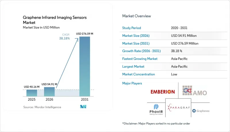
에 따르면 그래핀 적외선 이미징 센서 시장 규모는 2025년에 4,016만 달러로 평가되며, 2026년 5,491만 달러에서 2031년까지 2억 7,659만 달러에 달할 것으로 예측되고 있으며, 예측 기간(2026-2031년)에 CAGR은 38.18%에 달할 전망입니다.
글로벌 그래핀 적외선 이미징 센서 시장의 동향 및 인사이트
웨이퍼 상의 그래핀 집적 비용 감소
그래핀의 집적 비용은 센서 보급을 저해하는 주요 장벽이 되어 왔습니다. AMO GmbH는 2026년, EU의 2D 파일럿 라인 하에서 4차 멀티프로젝트 웨이퍼 생산을 시작했습니다. 이 프로그램을 통해 여러 설계 고객 간에 디바이스 비용을 분담함으로써 파운드리 등급 프로토타이핑 비용을 절감하고 있습니다. 2025년 연구에서는 3,200mm 생산 런에서 96-98%의 디바이스 수율이 보고되었으며, 재현성 있는 배치 처리가 가능함이 입증되었습니다. 또한 AMO사는 CMOS 백엔드의 열적 제약과 호환성을 유지하면서 확장 가능한 알루미늄 산화물 유전체 공정 경로에 대해서도 보고하고 있습니다. 따라서 그래핀 적외선 이미징 센서 시장에서는 완전히 독립된 제조 인프라를 필요로 하지 않고, 기존의 실리콘 제조 공정을 활용할 수 있습니다. 이를 통해 그래핀 적외선 이미징 센서 시장의 생산성 향상이 기대됩니다.
저비용 비냉각형 SWIR 이미징에 대한 수요
기존의 인듐-갈륨-비소(InGaAs) 기반 SWIR 센서는 대량 생산이 요구되는 많은 용도에서 여전히 고가였습니다. Emberion사는 2024년, 대량 생산시 단가 목표를 개당 50유로(개당 54달러)로 설정하는 초저비용 SWIR 센서를 발표했습니다. 이 회사의 웨이퍼 레벨 패키징 공정에서는 8인치 웨이퍼 1장당 최대 100개의 센서를 실장할 수 있습니다. 엠베리온은 2025년, 웨이퍼 전체에서 100%의 본딩 수율을 달성하며 초기 패키징 개발 및 시험 단계를 완료했습니다. 디바이스 비용의 감소로 인해 SWIR의 도입 범위는 자동차 시스템 및 소비자 가전 제품으로 확대될 가능성이 있습니다. 또한 그래핀 적외선 이미징 센서 시장도 이러한 생산량 증가에 따른 제조상의 학습 효과의 혜택을 누릴 것입니다. 이를 통해 그래핀 적외선 이미징 센서 시장에는 단가를 더욱 낮출 수 있는 새로운 길이 열리게 될 것입니다.
제한된 상업적 생산량
2026년에도 공급 능력은 그래핀 적외선 이미징 센서에 있으며, 여전히 제약 요인으로 작용하고 있습니다. 국방, 머신 비전, 자동차 분야의 고객 수요는 생산 처리량 증가 속도를 앞지르는 속도로 확대되고 있습니다. 엠벨리온(Emberion)사는 현재 수요가 공급을 크게 상회하고 있음을 밝히고, 공정 및 설비 투자에 새로운 자본을 투입하고 있습니다. 구리 성장 기판에서 센서 웨이퍼로 그래핀을 전사하는 공정에서는 결함이나 계면 불균일성이 발생할 가능성이 있습니다. 이 때문에 다른 공정 단계가 최적화되어 있더라도 웨이퍼당 높은 수율을 유지하기 어렵습니다. 공급업체가 생산 능력 확장을 완료하고 대량 공급을 보장할 수 있게 될 때까지 그래핀 적외선 이미징 센서 시장에서는 납기 지연이 발생할 가능성이 있습니다.
부문 분석
2025년 시점에 검출 메커니즘별로 보면 광전도형 및 포토게이팅형 검출기가 그래핀 적외선 이미징 센서 시장의 35.67%를 차지했습니다. 이 점유율은 GFET-양자점 플랫폼의 성숙도를 반영하고 있습니다. 양자점 흡수체는 그래핀 트랜지스터의 게이트 전압을 조절하여 검출기의 높은 응답성을 지원합니다. 200mm 웨이퍼 규모의 플랫폼에서는 400-1,800nm 파장 범위에서 105-106 V/W의 감도를 달성했습니다. 이 연구에서는 96%의 제조 수율도 보고되었습니다. 이 아키텍처는 상용 CMOS 판독 집적회로와 호환됩니다. 또한 백엔드 공정 온도에서 제조할 수 있으므로, 인듐갈륨비소(InGaAs) 제조에 사용되는 에피택셜 성장 공정의 일부를 생략할 수 있습니다. 또한 태양광발전 소자는 고정밀 단파장 적외선(SWIR) 분광법을 위한 제로 바이어스 방식을 제공합니다.
광열전 검출기는 2031년까지 40.74%라는 가장 높은 연평균 성장률(CAGR)을 기록할 것으로 예측됩니다. 이 검출기들은 그래핀의 제백 효과를 이용하여 적외선에 의해 발생하는 열 구배를 전압으로 변환합니다. 이를 통해 외부 바이어스나 게이트 전압 없이도 작동할 수 있습니다. 2025년에 개발된 150mm SOI(Silicon on Insulator) 플랫폼 기반의 플라즈몬 증강형 검출기는 4.2µm 파장에서 감도가 3배 향상되었습니다. 또한 25.6 kHz의 주파수 응답도 달성했습니다. 그래핀 및 육방정계 질화붕소(h-BN) 구조 역시 계면의 열 비대칭성을 이용하여 바이어스 없는 광전류를 발생시킵니다. 픽셀당 판독 소자 수를 줄임으로써 초점면 어레이의 비용을 절감할 수 있습니다. 보로메트릭 소자는 특수한 과학적 용도에서 여전히 중요하지만, 최고 성능을 발휘하기 위해서는 12 K 이하의 온도가 필요합니다.
2025년 시점에 파장대별로 보면 단파장 적외선(SWIR)은 그래핀 적외선 이미징 센서 시장의 32.34%를 차지했습니다. 이는 그래핀 이미징 분야에서 상업적으로 가장 성숙한 파장대입니다. Graphenea사의 그래핀을 활용한 SWIR 카메라에 대한 연구는 이러한 위치를 지원하고 있습니다. 출하되고 있는 가시광선·단파장 적외선(VIS-SWIR) 카메라 제품은 400-2,000 nm의 파장 범위를 커버하고 있습니다. 근적외선 디바이스 또한 뛰어난 기술적 성능을 보여주고 있습니다. 그래핀 나노리본과 알루미늄 산화물-실리콘 헤테로접합은 -6 V의 바이어스 조건에서 1,064 nm 파장에서 159.55 A/W의 감도와 2.01×10¹² 존스의 검출도를 달성했습니다. 이 연구에서는 자가 구동시 감도가 8.71 A/W라는 사실도 보고되었습니다. 이러한 성능은 기존 실리콘 카메라를 뛰어넘는 감도가 필요한 응용 분야를 지원하고 있습니다.
중파장 적외선은 2031년까지 연평균 성장률(CAGR)이 41.89%에 달해 가장 빠르게 성장하는 스펙트럼 범주가 될 것으로 예측됩니다. 국방용 센싱, 가스 감지 및 산업용 모니터링이 이러한 전망을 지원하고 있습니다. 2025년 나노하이브리드 검출기에 관한 연구에서는 HgTe 양자점과 그래핀을 사용하여 실온에서 2.4×10¹¹ 존스의 검출도를 달성했다고 보고되었습니다. 이 연구에서는 결정립 합체 성장법을 사용하여 표면 상태의 전하 트랩 문제를 해결했습니다. 유연한 HgTe 양자점 및 그래핀 소자는 반경 5.5 mm에서 반복적인 굽힘 시험을 거치더라도 성능을 유지했습니다. 장파장 적외선 분야에는 여전히 기술적으로 해결해야 할 과제가 남아 있습니다. 그럼에도 불구하고 실리콘 기판 위의 그래핀 및 리튬 니오브산 소자는 8.0µm 및 10.5µm 파장에서 95.9-187 kV/W의 감도를 달성했습니다.
지역별 분석
아시아태평양은 2025년에 34.65%의 지역 점유율을 차지할 것으로 예상되며, 2031년까지 연평균 성장률(CAGR) 41.12%로 성장할 것으로 전망됩니다. 중국은 도파관 집적 칩 및 포토닉 결정 강화 센서 등 그래핀 적외선 아키텍처 분야에서 탄탄한 연구 기반을 갖추고 있습니다. 한국은 포항 K-그래핀 파운드리(K-Graphene Foundry)를 통해 POSTECH 인근에 그래핀 제조 공유 설비를 구축하고 있으며, 2026-2030년 143억 원(1,040만 달러)의 지원이 예정되어 있습니다. 인도의 국방 현대화도 현지 사양에 부합하는 단파 적외선(SWIR) 및 중파 적외선(MWIR) 모듈의 수요를 지원하고 있습니다. 이러한 상황으로 인해 해당 지역은 중요한 고객 기반인 동시에 신흥 공급 거점으로도 자리매김하고 있습니다.
북미와 유럽은 여전히 기술 공급 측면에서 중심적인 역할을 하고 있습니다. 미국 국방부의 연구 프로그램과 SBIR(중소기업 혁신 연구) 보조금은 대학 연구에서 방위 인증에 이르기까지의 경로를 제공하고 있습니다. Paragraf사는 이 두 지역에서 사업을 운영하고 있으며, 2025년 시리즈 C 라운드에서 5,500만 달러를 조달했습니다. 이 중 3,500만 달러는 무바달라 캐피털(Mubadala Capital)의 투자입니다. 유럽에는 그래핀 플래그십 프로젝트, AMO의 2D 파일럿 라인, 핀란드에서 생산 활동을 펼치고 있는 엠베리온(Emberion)에 이르는 통합된 생태계가 존재합니다. 독일, 영국, 스페인, 프랑스, 핀란드 각국에는 그래핀 적외선 센싱 분야에서 상업 활동을 펼치는 조직이 있습니다.
남미, 중동 및 아프리카는 그래핀 적외선 이미징 센서 시장에서 규모는 작지만 변화하고 있는 분야입니다. 브라질은 INPE(국립우주연구소) 관련 기관 및 대학의 광학 프로그램을 통해 이 지역에서 가장 발전된 포토닉스 연구 기반을 보유하고 있지만, 2026년 시점에는 상업적인 그래핀 적외선 센서의 생산 능력은 확립되지 않았습니다. 중동은 제조 거점이라기보다는 투자 및 조달 센터로서 발전하고 있습니다. 파라그래프(Paragraph)사가 무바다라(Mubadala)사와 공동으로 계획하고 있는 UAE로의 사업 확장은 이러한 역할을 지원합니다. 사우디아라비아와 UAE는 감시 및 국경 경비용 이미징 시스템의 잠재적 구매처입니다. 아프리카에서는 농업, 환경, 자원 모니터링 용도에서 향후 수요가 예상됩니다.
기타 혜택:
- 엑셀 형식의 시장 예측(ME) 시트
- 3개월간의 애널리스트 지원
자주 묻는 질문
목차
제1장 서론
- 조사 전제조건과 시장 정의
- 조사 범위
제2장 조사 방법
제3장 개요
제4장 시장 구도
- 시장 개요
- 거시경제 요인이 시장에 미치는 영향
- 시장 성장 촉진요인
- 시장 성장 억제요인
- 업계 밸류체인 분석
- 규제 상황
- 기술 전망
- Porter's Five Forces 분석
제5장 시장 규모와 성장 예측
- 탐지 메커니즘별
- 스펙트럼 범위별
- 냉각 기술별
- 용도별
- 지역별
- 북미
- 미국
- 캐나다
- 멕시코
- 남미
- 브라질
- 아르헨티나
- 기타 남미 국가
- 유럽
- 독일
- 영국
- 프랑스
- 이탈리아
- 스페인
- 기타 유럽 국가
- 아시아태평양
- 중국
- 일본
- 인도
- 한국
- ASEAN
- 기타 아시아태평양 국가
- 중동 및 아프리카
- 중동
- 사우디아라비아
- 아랍에미리트
- 기타 중동 국가
- 아프리카
- 남아프리카공화국
- 이집트
- 기타 아프리카 국가
- 중동
- 북미
제6장 경쟁 구도
- 시장 집중도
- 전략적 동향
- 시장 점유율 분석
- 기업 개요
- Graphenea Semiconductor SL
- Emberion Limited
- AMO GmbH
- Paragraf Limited
- PhovIR Technologies Ltd
- Quantum Science Ltd
- Quantum Solutions
- Sony Semiconductor Solutions Corporation
- TriEye Ltd
- Lynred S.A.S.
- New Imaging Technologies S.A.
- Teledyne FLIR LLC
- SCD SemiConductor Devices
- Sensors Unlimited, Inc.
- BAE Systems plc
- Attollo Engineering, LLC
제7장 시장 기회와 향후 전망
KSA 26.10.29According to Mordor Intelligence, the graphene infrared imaging sensors market size was valued at USD 40.16 million in 2025 and estimated to grow from USD 54.91 million in 2026 to reach USD 276.59 million by 2031, at a CAGR of 38.18% during the forecast period (2026-2031).
Global Graphene Infrared Imaging Sensors Market Trends and Insights
Falling Graphene-On-Wafer Integration Costs
Graphene integration costs have been a central barrier to broader sensor adoption. AMO GmbH opened its fourth multi-project wafer run under the EU 2D Pilot Line in 2026. The program shares device costs among several design customers and reduces the cost of foundry-grade prototyping. A 2025 study reported a 96-98% device yield across 3,200 mm production runs, demonstrating reproducible batch processing. AMO also reported a scalable aluminum oxide dielectric route that remained compatible with CMOS back-end thermal limits. The graphene infrared imaging sensors market can therefore use existing silicon manufacturing flows without requiring entirely separate fabrication infrastructure. This improves the production case for the graphene infrared imaging sensors market.
Demand for Low-Cost Uncooled SWIR Imaging
Conventional indium gallium arsenide SWIR sensors have remained expensive for many volume-sensitive uses. Emberion introduced an ultra-low-cost SWIR sensor in 2024 with a production target of EUR 50 per unit (USD 54 per unit) at large volumes. Its wafer-level packaging process supports up to 100 sensors per 8-inch wafer. Emberion completed an initial packaging development and testing round with a 100% bond yield across a full wafer in 2025. Lower device costs could extend SWIR deployment into automotive systems and consumer devices. The graphene infrared imaging sensors market would also gain from the manufacturing learning effects associated with these higher unit volumes. This gives the graphene infrared imaging sensors market an additional route to lower unit costs.
Limited Commercial Production Volumes
Supply capacity remains a limiting issue for graphene infrared imaging sensors in 2026. Demand from defense, machine vision, and automotive customers has grown faster than production throughput. Emberion stated that current demand significantly exceeded supply and directed new capital toward process and equipment investment. Graphene transfer from copper growth substrates to sensor wafers can introduce defects and interface variation. This makes high per-wafer yield harder to sustain, even when other process stages are optimized. The graphene infrared imaging sensors market may face longer delivery periods until suppliers complete capacity expansion and can offer volume commitments.
Other drivers and restraints analyzed in the detailed report include:
- Expansion of AI-Enabled Machine Vision
- Growth in Defense and Automotive Night Vision
- Qualification Risk Against Mature InGaAs and MCT Sensors
For complete list of drivers and restraints, kindly check the Table Of Contents.
Segment Analysis
Photoconductive and photogating detectors accounted for 35.67% of the graphene infrared imaging sensors market share by detection mechanism in 2025. Their position reflects the maturity of GFET-quantum dot platforms. Quantum dot absorbers modulate the graphene transistor gate voltage and support high detector response. A 200 mm wafer-scale platform delivered responsivities of 105-106 V/W across the 400-1,800 nm range. The same work reported a 96% fabrication yield. This architecture aligns with commercial CMOS readout integrated circuits. It can be fabricated at back-end process temperatures, which avoids some epitaxial growth steps used in indium gallium arsenide production. Photovoltaic devices also offer a zero-bias route for precision SWIR spectroscopy.
Photothermoelectric detectors are projected to record the highest CAGR of 40.74% through 2031. They convert infrared-driven thermal gradients into voltage through graphene's Seebeck effect. This enables operation without external bias or gate voltage. A 2025 plasmon-enhanced detector on a 150 mm silicon-on-insulator platform achieved a 3-fold increase in responsivity at a wavelength of 4.2 µm. It also reached a 25.6 kHz frequency response. Graphene and hexagonal boron nitride structures have also generated bias-free photocurrent via interfacial thermal asymmetry. Fewer readout components per pixel can reduce focal-plane array cost. Bolometric devices remain relevant for specialized scientific uses, but their highest-performing forms need temperatures below 12 K.
Short-wave infrared held 32.34% of the graphene infrared imaging sensors market share by spectral range in 2025. It is the most commercially mature spectral category for graphene imaging. Graphenea's work on graphene-enabled SWIR cameras supports this position. Shipped VIS-SWIR camera products cover wavelengths from 400 to 2,000 nm. Near-infrared devices also show strong technical performance. A graphene nanoribbon and aluminum oxide silicon heterojunction achieved 159.55 A/W responsivity and 2.01 X 10¹² Jones detectivity at 1,064 nm under -6 V bias. The same study reported self-powered responsivity of 8.71 A/W. These capabilities support applications that require sensitivity beyond that of conventional silicon cameras.
Mid-wave infrared is projected to be the fastest-growing spectral category at a 41.89% CAGR through 2031. Defense sensing, gas detection, and industrial monitoring are supporting this outlook. A 2025 study on a 2025 nanohybrid detector reported a room-temperature detectivity of 2.4 X 10¹¹ Jones using HgTe quantum dots and graphene. The work addressed surface-state charge traps through a grain-coalescence growth approach. Flexible HgTe quantum dot and graphene devices maintained performance during repeated bending at a 5.5 mm radius. Long-wave infrared remains technically demanding. Graphene and lithium niobate devices nevertheless achieved 95.9-187 kV/W responsivity at 8.0 and 10.5 µm on silicon substrates.
Complete Report Scope:
- By Detection Mechanism
- Photovoltaic Detectors
- Photothermoelectric Detectors
- Photoconductive / Photogating Detectors
- Bolometric Detectors
- By Spectral Range
- Near-Infrared (NIR)
- Short-Wave Infrared (SWIR)
- Mid-Wave Infrared (MWIR)
- Long-Wave Infrared (LWIR)
- By Cooling Technology
- Uncooled
- Thermoelectrically Cooled
- Cryogenically Cooled
- By Application
- Industrial Inspection and Machine Vision
- Defense, Security and Surveillance
- Remote Sensing and Environmental Monitoring
- Scientific and Medical
- Other Applications
- By Geography
- North America
- United States
- Canada
- Mexico
- South America
- Brazil
- Argentina
- Rest of South America
- Europe
- Germany
- United Kingdom
- France
- Italy
- Spain
- Rest of Europe
- Asia-Pacific
- China
- Japan
- India
- South Korea
- ASEAN
- Rest of Asia-Pacific
- Middle East and Africa
- Middle East
- Saudi Arabia
- United Arab Emirates
- Rest of the Middle East
- Africa
- South Africa
- Egypt
- Rest of Africa
- Middle East
- North America
Geography Analysis
Asia-Pacific held 34.65% regional share in 2025 and is projected to grow at a 41.12% CAGR through 2031. China has a substantial research base in graphene infrared architectures, including waveguide-integrated chips and photonic crystal-enhanced sensors. South Korea is building shared graphene manufacturing capacity near POSTECH through the Pohang K-Graphene Foundry, with KRW 14.3 billion (USD 10.4 million) in support for 2026-2030. India's defense modernization also supports demand for locally compatible SWIR and MWIR modules. These conditions make the region both an important customer base and an emerging supply location.
North America and Europe remain central to the technology supply side. North American Department of Defense research programs and SBIR awards provide a path from university research to defense qualification. Paragraf operates across the two regions and raised USD 55 million in a 2025 Series C round, including USD 35 million from Mubadala Capital. Europe has an integrated ecosystem spanning Graphene Flagship projects, AMO's 2D Pilot Line, and Emberion's Finnish production activity. Germany, the United Kingdom, Spain, France, and Finland each host commercially active organizations in graphene infrared sensing.
South America, the Middle East and Africa represent a smaller but changing part of the graphene infrared imaging sensors market. Brazil has the region's most developed photonics research base through INPE-linked institutions and university optics programs, but no commercial graphene infrared sensor production capability had been established as of 2026. The Middle East is developing as an investment and procurement center rather than a manufacturing hub. Paragraf's planned UAE expansion with Mubadala points to this role. Saudi Arabia and the UAE are potential buyers of surveillance and border-security imaging systems. Africa may provide future demand for agricultural, environmental, and resource-monitoring applications.
- Graphenea Semiconductor SL
- Emberion Limited
- AMO GmbH
- Paragraf Limited
- PhovIR Technologies Ltd
- Quantum Science Ltd
- Quantum Solutions
- Sony Semiconductor Solutions Corporation
- TriEye Ltd
- Lynred S.A.S.
- New Imaging Technologies S.A.
- Teledyne FLIR LLC
- SCD SemiConductor Devices
- Sensors Unlimited, Inc.
- BAE Systems plc
- Attollo Engineering, LLC
Additional Benefits:
- The market estimate (ME) sheet in Excel format
- 3 months of analyst support
TABLE OF CONTENTS
1 INTRODUCTION
- 1.1 Study Assumptions and Market Definition
- 1.2 Scope of the Study
2 RESEARCH METHODOLOGY
3 EXECUTIVE SUMMARY
4 MARKET LANDSCAPE
- 4.1 Market Overview
- 4.2 Impact of Macroeconomic Factors on the Market
- 4.3 Market Drivers
- 4.3.1 Falling Cost of Graphene-on-Wafer Integration
- 4.3.2 Demand for Low-Cost Uncooled SWIR Imaging
- 4.3.3 Expansion of AI-Enabled Machine Vision
- 4.3.4 Growth in Defense and Automotive Night Vision
- 4.3.5 Wafer-Scale GFET-Quantum Dot Manufacturing
- 4.3.6 Edge Spectral Intelligence in Compact Devices
- 4.4 Market Restraints
- 4.4.1 Limited Commercial Production Volumes
- 4.4.2 Qualification Risk Versus Mature InGaAs and MCT Sensors
- 4.4.3 Graphene Transfer and Interface-Uniformity Variability
- 4.4.4 Limited Availability of Standardized Graphene Sensor Specifications
- 4.5 Industry Value Chain Analysis
- 4.6 Regulatory Landscape
- 4.7 Technological Outlook
- 4.8 Porter's Five Forces Analysis
- 4.8.1 Bargaining Power of Suppliers
- 4.8.2 Bargaining Power of Buyers
- 4.8.3 Threat of New Entrants
- 4.8.4 Threat of Substitutes
- 4.8.5 Competitive Rivalry
5 MARKET SIZE AND GROWTH FORECASTS (VALUE)
- 5.1 By Detection Mechanism
- 5.1.1 Photovoltaic Detectors
- 5.1.2 Photothermoelectric Detectors
- 5.1.3 Photoconductive / Photogating Detectors
- 5.1.4 Bolometric Detectors
- 5.2 By Spectral Range
- 5.2.1 Near-Infrared (NIR)
- 5.2.2 Short-Wave Infrared (SWIR)
- 5.2.3 Mid-Wave Infrared (MWIR)
- 5.2.4 Long-Wave Infrared (LWIR)
- 5.3 By Cooling Technology
- 5.3.1 Uncooled
- 5.3.2 Thermoelectrically Cooled
- 5.3.3 Cryogenically Cooled
- 5.4 By Application
- 5.4.1 Industrial Inspection and Machine Vision
- 5.4.2 Defense, Security and Surveillance
- 5.4.3 Remote Sensing and Environmental Monitoring
- 5.4.4 Scientific and Medical
- 5.4.5 Other Applications
- 5.5 By Geography
- 5.5.1 North America
- 5.5.1.1 United States
- 5.5.1.2 Canada
- 5.5.1.3 Mexico
- 5.5.2 South America
- 5.5.2.1 Brazil
- 5.5.2.2 Argentina
- 5.5.2.3 Rest of South America
- 5.5.3 Europe
- 5.5.3.1 Germany
- 5.5.3.2 United Kingdom
- 5.5.3.3 France
- 5.5.3.4 Italy
- 5.5.3.5 Spain
- 5.5.3.6 Rest of Europe
- 5.5.4 Asia-Pacific
- 5.5.4.1 China
- 5.5.4.2 Japan
- 5.5.4.3 India
- 5.5.4.4 South Korea
- 5.5.4.5 ASEAN
- 5.5.4.6 Rest of Asia-Pacific
- 5.5.5 Middle East and Africa
- 5.5.5.1 Middle East
- 5.5.5.1.1 Saudi Arabia
- 5.5.5.1.2 United Arab Emirates
- 5.5.5.1.3 Rest of the Middle East
- 5.5.5.2 Africa
- 5.5.5.2.1 South Africa
- 5.5.5.2.2 Egypt
- 5.5.5.2.3 Rest of Africa
- 5.5.5.1 Middle East
- 5.5.1 North America
6 COMPETITIVE LANDSCAPE
- 6.1 Market Concentration
- 6.2 Strategic Moves
- 6.3 Market Share Analysis
- 6.4 Company Profiles (includes Global Level Overview, Market Level Overview, Core Segments, Financials as available, Strategic Information, Market Rank/Share, Products and Services, Recent Developments)
- 6.4.1 Graphenea Semiconductor SL
- 6.4.2 Emberion Limited
- 6.4.3 AMO GmbH
- 6.4.4 Paragraf Limited
- 6.4.5 PhovIR Technologies Ltd
- 6.4.6 Quantum Science Ltd
- 6.4.7 Quantum Solutions
- 6.4.8 Sony Semiconductor Solutions Corporation
- 6.4.9 TriEye Ltd
- 6.4.10 Lynred S.A.S.
- 6.4.11 New Imaging Technologies S.A.
- 6.4.12 Teledyne FLIR LLC
- 6.4.13 SCD SemiConductor Devices
- 6.4.14 Sensors Unlimited, Inc.
- 6.4.15 BAE Systems plc
- 6.4.16 Attollo Engineering, LLC
7 MARKET OPPORTUNITIES AND FUTURE OUTLOOK
- 7.1 White-Space and Unmet-Need Assessment


