|
시장보고서
상품코드
2036335
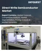
다이렉트 라이트 반도체 시장 규모, 점유율 및 성장 분석 : 기술/장비 유형별, 재료 유형별, 용도별, 지역별 - 업계 예측(2026-2033년)Direct Write Semiconductor Market Size, Share, and Growth Analysis, By Technology / Equipment Type (Laser Direct Write Systems, Electron Beam Direct Write Systems), By Material Type, By Application, By Region - Industry Forecast 2026-2033 |
||||||

세계의 다이렉트 라이트 반도체 시장 규모는 2024년에 58억 2,000만 달러로 평가되며, 2025년 66억 6,000만 달러에서 2033년까지 196억 9,000만 달러로 확대하며, 예측 기간(2026-2033년)에 CAGR 14.5%로 성장할 것으로 전망되고 있습니다.
전 세계 다이렉트 라이트 반도체 시장은 기능성 소재를 기판에 직접 패턴 형성할 수 있는 능력으로 포토마스크가 불필요해짐에 따라 주목받고 있습니다. 이 기술은 개발 주기를 단축하고 금형 비용을 절감하는 동시에, 특히 비평면 및 유연한 응용 분야에서 이질적인 통합을 촉진합니다. OEM 업체들은 제품의 복잡성 증가와 시장 출시 시간 단축에 대한 압박에 직면하여 마스크리스 및 소량 생산 방식으로 전환하고 있습니다. 고해상도 인쇄 기술의 발전과 나노입자 은, 구리 등 기능성 잉크의 발전으로 응용 범위가 넓어지고, 플렉서블 안테나 및 항공우주용 센서에 대한 혁신적인 솔루션이 가능해졌습니다. 또한 AI의 통합으로 패턴의 정확성과 일관성이 향상되어 생산 공정의 효율성이 크게 향상되었습니다. 이러한 융합은 대량 맞춤화 및 지역 밀착형 제조의 기회를 창출하고 시장 성장을 촉진하고 있습니다.
세계의 다이렉트 라이트 반도체 시장 촉진요인
세계의 다이렉트 라이트 반도체 시장은 패터닝의 정확성과 적응성을 향상시킨 마스크리스 리소그래피 기술의 눈부신 발전에 힘입어 성장하고 있습니다. 이러한 진화를 통해 제조업체는 복잡한 칩 설계에 다이렉트 라이트 공정을 적용하면서도 필요한 공정 단계 수를 최소화할 수 있게 되었습니다. 그 결과, 고가의 포토마스크에 대한 의존도를 낮추고, 개발 단계에서의 빠른 반복이 가능해져 궁극적으로 혁신을 가속화할 수 있게 되었습니다. 장비의 정밀도와 빔 제어 기술이 향상됨에 따라 특수한 소량 생산에서 직사광법은 점점 더 매력적으로 변하고 있으며, 다양한 틈새 반도체 응용 분야에서 채택이 확대되고 있으며, 공급업체들이 공정 통합과 장비 최적화에 집중하도록 유도하고 있습니다.
세계의 다이렉트 라이트 반도체 시장 억제요인
세계의 다이렉트 라이트 반도체 시장은 성장을 저해하는 몇 가지 중대한 도전에 직면해 있습니다. 첨단 직사광선 장비를 도입하기 위해 필요한 막대한 설비 투자에 더해, 이러한 시스템의 운영 및 유지보수에 필요한 전문적 노하우가 많은 제조업체들에게 장벽이 되고 있습니다. 높은 초기 비용은 효율성과 비용 효율성을 중시하는 대량 생산 시설에 장벽이 되는 경우가 많으며, 이 기술의 사용은 주로 틈새 시장이나 연구 지향적 용도로만 제한되어 있습니다. 또한 기존 생산 라인에 새로운 장비를 도입하려면 철저한 공정 검증과 직원에 대한 추가 교육이 필요하므로 설치 시간과 인지된 위험이 더욱 증가합니다. 이러한 재정적, 운영적 제약은 기술적 이점에도 불구하고 결국 광범위한 채택을 제한하고 전체 시장 확대를 지연시키고 있습니다.
세계 다이렉트 라이트 반도체 시장 동향
세계의 직하형 반도체 시장에서는 첨단 패키징 통합에 초점을 맞춘 두드러진 시장 추세를 볼 수 있습니다. 이러한 변화는 팹리스 설계자, OSAT, 웨이퍼 팹 간의 협업을 촉진하고, 이종 시스템 인 패키지(SiP) 솔루션의 개발을 주도하고 있습니다. 기능 밀도와 상호 연결 성능에 대한 중요성이 높아지면서 칩과 기판 설계에 대한 공동 최적화 접근법이 요구되고 있습니다. 그 결과, 웨이퍼 레벨 공정과 특수 본딩 기술의 채택이 증가하고 있으며, 공급망의 보다 긴밀한 연계가 필요하게 되었습니다. 이러한 추세는 부가가치를 높일 수 있는 기회를 창출할 뿐만 아니라, 다양한 구성 요소 생태계에서 상호 운용성을 보장하기 위해 엄격한 교차 도메인 테스트와 표준화된 관행의 중요성을 강조하고 있습니다.
자주 묻는 질문
목차
서론
조사 방법
개요
시장 역학과 전망
주요 시장 인사이트
세계의 다이렉트 라이트 반도체 시장 규모 : 기술/장비 유형별
세계의 다이렉트 라이트 반도체 시장 규모 : 소재 유형별
세계의 다이렉트 라이트 반도체 시장 규모 : 용도별
세계의 다이렉트 라이트 반도체 시장 규모 : 지역별
경쟁 정보
주요 기업 개요
결론과 제안
KSA 26.05.26Global Direct Write Semiconductor Market size was valued at USD 5.82 Billion in 2024 and is poised to grow from USD 6.66 Billion in 2025 to USD 19.69 Billion by 2033, growing at a CAGR of 14.5% during the forecast period (2026-2033).
The global direct write semiconductor market is gaining traction due to its capacity for patterning functional materials directly onto substrates, eliminating the need for photomasks. This technology accelerates development cycles and reduces tooling costs while facilitating heterogeneous integration, particularly for nonplanar and flexible applications. As OEMs face increasing product complexity and time-to-market pressures, they are moving toward maskless, low-volume production methods. The evolution of high-resolution printing techniques and advancements in functional inks, like nanoparticle silver and copper, broaden application possibilities, enabling innovative solutions for flexible antennas and aerospace sensors. Additionally, the integration of AI enhances patterning precision and consistency, significantly improving the efficiency of production processes. This convergence is driving opportunities in mass customization and localized manufacturing, fostering market growth.
Top-down and bottom-up approaches were used to estimate and validate the size of the Global Direct Write Semiconductor market and to estimate the size of various other dependent submarkets. The research methodology used to estimate the market size includes the following details: The key players in the market were identified through secondary research, and their market shares in the respective regions were determined through primary and secondary research. This entire procedure includes the study of the annual and financial reports of the top market players and extensive interviews for key insights from industry leaders such as CEOs, VPs, directors, and marketing executives. All percentage shares split, and breakdowns were determined using secondary sources and verified through Primary sources. All possible parameters that affect the markets covered in this research study have been accounted for, viewed in extensive detail, verified through primary research, and analyzed to get the final quantitative and qualitative data.
Global Direct Write Semiconductor Market Segments Analysis
Global direct write semiconductor market is segmented by technology / equipment type, material type, application and region. Based on technology / equipment type, the market is segmented into Laser Direct Write Systems, Electron Beam Direct Write Systems, Thermal Scanning Probe Lithography and Material Deposition Systems. Based on material type, the market is segmented into Conductive Materials, Semiconductor Materials, Dielectric and Insulating Materials and Functional Composite Materials. Based on application, the market is segmented into Advanced Packaging and Interconnects, Flexible and Printed Electronics, MEMS and Sensors and Biomedical and Healthcare Devices. Based on region, the market is segmented into North America, Europe, Asia Pacific, Latin America and Middle East & Africa.
Driver of the Global Direct Write Semiconductor Market
The Global Direct Write Semiconductor market is driven by significant advancements in maskless lithography techniques, which have enhanced patterning accuracy and adaptability. This evolution enables manufacturers to implement direct write processes on intricate chip designs while minimizing the number of required process steps. Consequently, there is less dependence on costly photomasks, facilitating quicker iterations during the development phase, which ultimately accelerates innovation. With improvements in equipment precision and beam control technologies, direct write methods are increasingly appealing for specialized and low-volume production, prompting wider adoption across various niche semiconductor applications and encouraging suppliers to focus on process integration and tool optimization.
Restraints in the Global Direct Write Semiconductor Market
The Global Direct Write Semiconductor market faces several considerable challenges that hinder its growth. The substantial capital investment needed to acquire advanced direct write equipment, coupled with the specialized expertise required to operate and maintain these systems, creates obstacles for many manufacturers. High initial costs often deter high-volume fabrication facilities that emphasize efficiency and cost-effectiveness, restricting the technology mainly to niche or research-oriented applications. Moreover, incorporating new equipment into established production lines necessitates thorough process validation and additional training for personnel, further increasing setup times and perceived risks. These financial and operational constraints ultimately limit widespread adoption and slow the overall expansion of the market, despite its technological benefits.
Market Trends of the Global Direct Write Semiconductor Market
The Global Direct Write Semiconductor market is witnessing a notable market trend focused on advanced packaging integration. This shift is fostering collaborative efforts among fabless designers, OSATs, and wafer fabs, driving the development of heterogeneous system-in-package solutions. The increased emphasis on functional density and interconnect performance is prompting a co-optimization approach to chip and substrate design. As a result, there is a growing adoption of wafer-level processes and specialized bonding techniques, necessitating closer supply-chain coordination. This trend not only creates opportunities for enhanced value propositions but also highlights the importance of rigorous cross-domain testing and standardized practices for ensuring interoperability in diverse component ecosystems.
Table of Contents
Introduction
- Objectives of the Study
- Market Definition & Scope
Research Methodology
- Research Process
- Secondary & Primary Data Methods
- Market Size Estimation Methods
Executive Summary
- Global Market Outlook
- Key Market Highlights
- Segmental Overview
- Competition Overview
Market Dynamics & Outlook
- Macro-Economic Indicators
- Drivers & Opportunities
- Restraints & Challenges
- Supply Side Trends
- Demand Side Trends
- Porters Analysis & Impact
- Competitive Rivalry
- Threat of Substitute
- Bargaining Power of Buyers
- Threat of New Entrants
- Bargaining Power of Suppliers
Key Market Insights
- Key Success Factors
- Market Impacting Factors
- Top Investment Pockets
- Ecosystem Mapping
- Market Attractiveness Index 2025
- PESTEL Analysis
- Regulatory Landscape
Global Direct Write Semiconductor Market Size by Technology / Equipment Type & CAGR (2026-2033)
- Market Overview
- Laser Direct Write Systems
- Electron Beam Direct Write Systems
- Thermal Scanning Probe Lithography
- Material Deposition Systems
Global Direct Write Semiconductor Market Size by Material Type & CAGR (2026-2033)
- Market Overview
- Conductive Materials
- Semiconductor Materials
- Dielectric and Insulating Materials
- Functional Composite Materials
Global Direct Write Semiconductor Market Size by Application & CAGR (2026-2033)
- Market Overview
- Advanced Packaging and Interconnects
- Flexible and Printed Electronics
- MEMS and Sensors
- Biomedical and Healthcare Devices
Global Direct Write Semiconductor Market Size & CAGR (2026-2033)
- North America (Technology / Equipment Type, Material Type, Application)
- US
- Canada
- Europe (Technology / Equipment Type, Material Type, Application)
- Germany
- Spain
- France
- UK
- Italy
- Rest of Europe
- Asia Pacific (Technology / Equipment Type, Material Type, Application)
- China
- India
- Japan
- South Korea
- Rest of Asia-Pacific
- Latin America (Technology / Equipment Type, Material Type, Application)
- Mexico
- Brazil
- Rest of Latin America
- Middle East & Africa (Technology / Equipment Type, Material Type, Application)
- GCC Countries
- South Africa
- Rest of Middle East & Africa
Competitive Intelligence
- Top 5 Player Comparison
- Market Positioning of Key Players, 2025
- Strategies Adopted by Key Market Players
- Recent Developments in the Market
- Company Market Share Analysis, 2025
- Company Profiles of All Key Players
- Company Details
- Product Portfolio Analysis
- Company's Segmental Share Analysis
- Revenue Y-O-Y Comparison (2023-2025)
Key Company Profiles
- ASML
- Company Overview
- Business Segment Overview
- Financial Updates
- Key Developments
- Applied Materials
- Company Overview
- Business Segment Overview
- Financial Updates
- Key Developments
- KLA Corporation
- Company Overview
- Business Segment Overview
- Financial Updates
- Key Developments
- Heidelberg Instruments
- Company Overview
- Business Segment Overview
- Financial Updates
- Key Developments
- EV Group (EVG)
- Company Overview
- Business Segment Overview
- Financial Updates
- Key Developments
- Suss MicroTec
- Company Overview
- Business Segment Overview
- Financial Updates
- Key Developments
- Screen Holdings
- Company Overview
- Business Segment Overview
- Financial Updates
- Key Developments
- Orbotech (KLA)
- Company Overview
- Business Segment Overview
- Financial Updates
- Key Developments
- Advantest
- Company Overview
- Business Segment Overview
- Financial Updates
- Key Developments
- Micro-Electronics
- Company Overview
- Business Segment Overview
- Financial Updates
- Key Developments
- Nano-Master
- Company Overview
- Business Segment Overview
- Financial Updates
- Key Developments
- Micro-Link
- Company Overview
- Business Segment Overview
- Financial Updates
- Key Developments
- Nikon
- Company Overview
- Business Segment Overview
- Financial Updates
- Key Developments
- Canon
- Company Overview
- Business Segment Overview
- Financial Updates
- Key Developments
- Fuji Film
- Company Overview
- Business Segment Overview
- Financial Updates
- Key Developments
- Siconnex
- Company Overview
- Business Segment Overview
- Financial Updates
- Key Developments
- Raith
- Company Overview
- Business Segment Overview
- Financial Updates
- Key Developments
- JEOL
- Company Overview
- Business Segment Overview
- Financial Updates
- Key Developments
- MGI Tech
- Company Overview
- Business Segment Overview
- Financial Updates
- Key Developments
- Oxford Instruments
- Company Overview
- Business Segment Overview
- Financial Updates
- Key Developments