|
시장보고서
상품코드
1881235
반도체 제조 장비 시장 : 리소그래피, 웨이퍼 표면 처리, 웨이퍼 세정, 증착, 조립, 패키징, 다이싱, 계측, 본딩, 웨이퍼 검사, IC 검사, 메모리, 로직, 디스크리트, 아날로그별, 예측(-2032년)Semiconductor Manufacturing Equipment Market by Lithography, Wafer Surface Conditioning, Wafer Cleaning, Deposition, Assembly & Packaging, Dicing, Metrology, Bonding, Wafer Testing/IC Testing, Memory, Logic, Discrete, Analog - Global Forecast to 2032 |
||||||
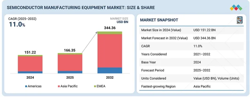
세계 반도체 제조장비 시장 규모는 2025년 1,663억 5,000만 달러, 2032년까지 3,443억 6,000만 달러에 이를 것으로 예측되며, CAGR은 11.0%를 나타낼 전망입니다.
자동차용 반도체 부문의 급속한 성장은 2025년 반도체 제조 장비 시장의 주요 촉진요인으로 부상하고 있습니다. 자동차 산업이 전기, 자율주행, 첨단 연결성, 소프트웨어 정의 아키텍처로 전환하는 동안 마이크로컨트롤러, PMIC, 센서, ADAS 프로세서를 포함한 고신뢰성 반도체 부품에 대한 수요는 급격히 증가하고 있습니다.
| 조사 범위 | |
|---|---|
| 조사 기간 | 2021-2032년 |
| 기준 연도 | 2024년 |
| 예측 기간 | 2025-2032년 |
| 단위 | 10억 달러 |
| 부문 | 제조 공정, 최종 사용자, 전 공정 장비, 후 공정 장비, 지역 |
| 대상 지역 | 북미, 유럽, 아시아태평양 및 기타 지역 |
전기자동차(EV)로의 급속한 전환과 1대당 반도체 탑재량 증가로 인해 트랙션 인버터, 배터리 관리 시스템, 파워 일렉트로닉스, 센싱 모듈, ADAS 플랫폼 등에 사용되는 첨단 칩 수요가 대폭 증가하고 있습니다. 자동차 제조업체와 Tier 1 공급업체는 자동차 등급 반도체 생산을 위해 팹 생산 능력을 확대하고 기존 라인을 업그레이드하고 있으며, 리소그래피, 증착, 에칭, 측정 및 검사 도구와 같은 중요한 장비에 대한 투자를 직접 촉진하고 있습니다. 자동차 응용 분야에서 엄격한 성능, 신뢰성 및 추적성 요구 사항을 바탕으로 이 부문은 정밀 제조와 견고한 품질 관리를 중시하며 자동차 인증 툴 세트를 갖춘 반도체 제조 장비 공급업체에게 혜택을 제공합니다.

"OSAT 기업이 예측 기간에 최고의 CAGR을 기록할 전망입니다."
OSAT 기업은 업계가 첨단 패키징 및 고밀도 검사 요건으로 빠르게 전환하는 핵심에 있기 때문에 예측 기간에 가장 높은 CAGR을 나타낼 것으로 예측됩니다. 칩 설계가 AI/ML, HPC, 5G, 자율주행, 이기종 통합을 지원하는 방향으로 진화함에 따라 2.5D/3D 패키징, 팬아웃 웨이퍼 레벨 패키징, 시스템 임패키징(SiP), 고성능 자동검사장비(ATE) 등 선진 후공정에 대한 수요는 계속 급증하고 있습니다.
팹리스 기업은 비용 절감과 시장 투입의 가속을 목적으로 조립·검사 공정의 아웃소싱을 증가시키고 있으며, 이에 따라 OSAT 기업은 생산 능력의 확대와 첨단 장비의 채택을 강요받고 있습니다. 또한, 미세화의 진행, 칩렛 기반 아키텍처의 채택, 패키징 주도의 성능 향상으로의 전환이 OSAT 투자를 크게 밀어 올리고 있습니다. 이러한 요인으로 인해 최종 사용자별로는 OSAT 기업이 반도체 제조장비 시장에서 가장 성장이 빠른 부문이 되고 있습니다.
"검사장비가 2024년 반도체 제조후 공정장비 시장을 견인했습니다."
검사 장비는 반도체 제조 후 공정 장비 시장에서 가장 큰 점유율을 차지합니다. 이는 모든 반도체 장비가 출하 전에 기능 정확도, 성능 신뢰성 및 결함 없는 동작을 보장하기 위해 여러 검사 단계를 거쳐야 하기 때문입니다. I/O 수 증가, 미세화, 칩렛 아키텍처, 첨단 패키징 형식 등에 의해 칩의 복잡화가 진행됨에 따라 종합적인 전기적 검사, 기능 검사, 번인 검사, 시스템 레벨 검사에 대한 요구가 크게 증가하고 있습니다.
게다가 AI 가속기, 자동차 전자, 산업 자동화, 5G 등의 용도의 상승은 매우 높은 신뢰성과 안전 기준을 요구하고 검사 강도와 범위 요구 사항을 더욱 높여줍니다. 디바이스 고장에 드는 비용이 급격히 상승했기 때문에 엄격한 검사는 반도체 제조업체에게 필수적인 공정이 되고 있습니다. 결과적으로 OSAT, IDM, 팹리스 기업은 첨단 자동검사장비(ATE), 프로빙시스템, 검사기술에 대한 투자를 지속적으로 하고 있으며, 이로써 반도체 제조후 공정장비 시장에서 검사장비의 주도적 지위가 확고해집니다.
이 보고서는 세계 반도체 제조 장비 시장에 대한 조사 분석을 통해 주요 촉진요인 및 억제요인, 경쟁 구도, 미래 동향 등의 정보를 제공합니다.
자주 묻는 질문
목차
제1장 서론
제2장 주요 요약
제3장 중요한 지견
- 반도체 제조 장비 시장 : 기업에게 매력적인 기회
- 반도체 제조 장비 시장 : 최종사용자별
- 반도체 제조 장비 시장 : 전공정장비별
- 반도체 제조 장비 시장 : 지역별
제4장 시장 개요
- 소개
- 시장 역학
- 성장 촉진요인
- 억제요인
- 기회
- 과제
- 언멧 요구와 화이트 스페이스
- 연계 시장 및 교차 산업 기회
- Tier 1/2/3 기업의 전략적 움직임
제5장 업계 동향
- Porter's Five Forces 분석
- 거시경제지표
- 소개
- GDP의 동향과 예측
- 세계의 파운드리 업계 동향
- 세계의 IDM 업계 동향
- 세계의 OSAT 업계 동향
- 밸류체인 분석
- 생태계 분석
- 가격 설정 분석
- 주요 기업이 제공하는 전 공정 리소그래피 장비의 평균 판매 가격의 동향 : 유형별(2021년-2024년)
- 표준 리소그래피 장비의 평균 판매 가격의 동향 : 지역별(2021년-2024년)
- 무역 분석
- 수입 시나리오(HS 코드 848620)
- 수출 시나리오(HS 코드 848620)
- 주요 컨퍼런스 및 이벤트(2025년-2026년)
- 고객사업에 영향을 주는 동향/혼란
- 투자 및 자금조달 시나리오
- 사례 연구 분석
- 반도체 제조장비 시장에 대한 2025년 미국 관세의 영향
- 소개
- 주요 관세율
- 가격의 영향 분석
- 국가/지역에 미치는 영향
- 최종 사용자에게 미치는 영향
제6장 기술의 진보, AI에 의한 영향, 특허, 혁신 및 미래의 용도
- 주요 신기술
- 극단 자외선(EUV) 리소그래피
- 웨이퍼 본딩
- 보완 기술
- 기술/제품 로드맵
- 특허 분석
- 반도체 제조장비 시장에 대한 AI/생성형 AI의 영향
- 주요 이용 사례와 시장의 장래성
- 반도체 제조 장비 시장에서의 OEM 모범 사례
- 반도체 제조 장비 시장에서의 AI 도입에 관한 사례 연구
- 상호 연결된 생태계와 시장 기업에 미치는 영향
- AI/생성형 AI 통합 반도체 제조 장비의 채택에 대한 고객의 준비 상황
제7장 지역의 정세, 지속가능성에 관한 대처
- 지역 규제 및 규정 준수
- 규제기관, 정부기관, 기타 조직
- 업계 표준
- 지속가능성에 대한 노력
- 지속가능성 대처에 대한 규제정책의 영향
- 인증, 라벨, 환경 기준
제8장 고객정세와 구매행동
- 의사결정 프로세스
- 구매 프로세스에 참여하는 주요 이해관계자와 그 평가 기준
- 구매 프로세스의 주요 이해 관계자
- 구입 기준
- 채택 장벽과 내부 과제
- 다양한 최종 사용자의 언멧 요구
- 시장의 수익성
제9장 반도체 제조 장비에 있어서의 웨이퍼의 유형의 개관
- 소개
- 실리콘(SI)
- 실리콘 카바이드(SIC)
- 질화갈륨(GAN)
- 비소갈륨(GAAS)
- 기타 웨이퍼 유형
제10장 반도체 제조 장비의 최종 제품
- 소개
- 메모리
- 논리 디바이스
- MPU
- CPU
- GPU
- DSP
- 기타
- 이산 소자
- 아날로그 IC
- 기타 최종 제품
제11장 반도체 제조 장비에 있어서의 다양한 IC의 차원
- 소개
- 2D IC
- 2.5D IC
- 3D IC
제12장 반도체 제조 장비로 처리되는 웨이퍼의 사이즈
- 소개
- 150mm 이하
- 200mm
- 300mm
제13장 반도체 제조 장비 시장 : 제조 공정별
- 소개
- 전공정
- 후공정
- 기타 공정
제14장 반도체 제조 장비 시장 : 전공정 장비별
- 소개
- 리소그래피 장비
- 증착 장비
- 웨이퍼 표면 처리 장비
- 웨이퍼 세정 장비
- 계측·검사 장비
- 기타 전공정 장비
제15장 반도체 제조 장비 시장 : 후공정 장비별
- 소개
- 포장
- 다이싱
- 본딩
- 웨이퍼 검사/IC 검사
제16장 반도체 제조 장비 시장 : 최종 사용자별
- 소개
- 파운드리
- IDMS
- OSAT기업
- 기타 최종 사용자
제17장 반도체 제조 장비 시장 : 지역별
- 소개
- 아메리카
- 미국
- 기타 아메리카
- 아시아태평양
- 중국
- 일본
- 한국
- 대만
- 인도
- 기타 아시아태평양
- 유럽·중동 및 아프리카
- 유럽
- 중동 및 아프리카
제18장 경쟁 구도
- 개요
- 주요 참가 기업의 전략/강점(2024년-2025년)
- 수익 분석(2020년-2024년)
- 시장 점유율 분석(2024년)
- 기업 평가 및 재무 지표
- 제품 비교
- 기업 평가 매트릭스: 주요 기업(2024년)
- 기업의 평가 매트릭스: 스타트업/중소기업(2024년)
- 경쟁 시나리오
제19장 기업 프로파일
- 소개
- 주요 기업
- APPLIED MATERIALS, INC.
- ASML
- TOKYO ELECTRON LIMITED
- LAM RESEARCH CORPORATION
- KLA CORPORATION
- SCREEN HOLDINGS CO., LTD.
- TERADYNE INC.
- ZEISS GROUP
- ADVANTEST CORPORATION
- HITACHI HIGH-TECH CORPORATION
- PLASMA-THERM
- 기타 기업
- ASM INTERNATIONAL
- EV GROUP(EVG)
- ONTO INNOVATION
- NORDSON CORPORATION
- ADT-ADVANCED DICING TECHNOLOGIES
- BENEQ
- CVD EQUIPMENT CORPORATION
- EUGENE TECHNOLOGY CO. LTD.
- NIKON CORPORATION
- SEMICONDUCTOR EQUIPMENT CORP.
- SENTECH INSTRUMENTS GMBH
- CANON INC.
- KOKUSAI ELECTRIC CORPORATION
- SEMES
- FORMFACTOR
- 최종 사용자
- FOUNDRIES
- IDM FIRMS
- OSAT COMPANIES
제20장 조사 방법
제21장 부록
SHW 25.12.11The global semiconductor manufacturing equipment market is projected to grow from USD 166.35 billion in 2025 to USD 344.36 billion by 2032, at a CAGR of 11.0%. The rapid acceleration of the automotive semiconductor sector is emerging as a major driver of the semiconductor manufacturing equipment market in 2025. As the automotive industry transitions toward electrification, autonomous driving, enhanced connectivity, and software-defined architectures, demand for high-reliability semiconductor components, including microcontrollers, power-management ICs, sensors, and ADAS processors, continues to rise sharply.
| Scope of the Report | |
|---|---|
| Years Considered for the Study | 2021-2032 |
| Base Year | 2024 |
| Forecast Period | 2025-2032 |
| Units Considered | Value (USD Billion) |
| Segments | By Manufacturing Phase, End User, Front-end Equipment, Back-end Equipment and Region |
| Regions covered | North America, Europe, APAC, RoW |
The rapid shift toward EVs and higher semiconductor content per vehicle is substantially increasing demand for advanced chips used in traction inverters, battery-management systems, power electronics, sensing modules, and ADAS platforms. Automakers and tier-one suppliers are expanding fab capacity and upgrading existing lines to produce automotive-grade semiconductors, directly boosting investments in critical equipment such as lithography, deposition, etch, metrology, and inspection tools. Given the stringent performance, reliability, and traceability requirements in automotive applications, the segment places strong emphasis on precision manufacturing and robust quality control, benefiting semiconductor manufacturing equipment suppliers with automotive-qualified toolsets.
"OSAT Companies to Record Highest CAGR During Forecast Period"
OSAT companies are expected to record the highest CAGR during the forecast period because they are at the center of the industry's rapid shift toward advanced packaging and high-density testing requirements. As chip designs evolve to support AI/ML, HPC, 5G, automotive autonomy, and heterogeneous integration, the demand for sophisticated backend processes such as 2.5D/3D packaging, fan-out wafer-level packaging, system-in-package (SiP), and high-performance automated test equipment continues to surge.
Fabless companies are increasingly outsourcing assembly and testing to reduce costs and accelerate time-to-market, prompting OSATs to expand their capacity and adopt more advanced equipment. Furthermore, increased miniaturization, the adoption of chiplet-based architectures, and the transition toward packaging-driven performance improvements are significantly boosting OSAT investments. Collectively, these factors position OSAT companies as the fastest-growing segment in the semiconductor manufacturing equipment market based on end users.
"Testing Equipment Led Semiconductor Manufacturing Back-end Equipment Market in 2024"
Testing equipment holds the largest share of the back-end semiconductor manufacturing equipment market because every semiconductor device must undergo multiple mandatory test stages to ensure functional accuracy, performance reliability, and defect-free operation before shipment. As chips become more complex, with higher I/O counts, smaller geometries, chiplet architectures, and advanced packaging formats, the need for comprehensive electrical, functional, burn-in, and system-level testing increases significantly.
Moreover, the rise of applications such as AI accelerators, automotive electronics, industrial automation, and 5G requires extremely high reliability and safety standards, further increasing the intensity and coverage requirements of testing. The cost of device failure has risen sharply, making robust testing a non-negotiable step for semiconductor manufacturers. As a result, OSATs, IDMs, and fabless companies consistently invest in advanced automated test equipment (ATE), probing systems, and inspection technologies, thereby solidifying the leading position of testing equipment in the back-end semiconductor manufacturing equipment market.
"China to Dominate Asia Pacific Semiconductor Manufacturing Equipment Market throughout Forecast Period"
China holds the largest share of the semiconductor manufacturing equipment market due to its aggressive national push to expand domestic semiconductor production capacity and reduce dependence on foreign chip suppliers. The country has been investing heavily in new fabs, equipment procurement, and advanced manufacturing infrastructure as part of government-led initiatives, such as "Made in China 2025" and successive Five-year Plans, which prioritize semiconductor self-sufficiency.
China also hosts one of the world's fastest-growing ecosystems of foundries, memory manufacturers, and OSAT companies, such as JCET and Tongfu Microelectronics, driving continuous equipment purchases for capacity expansion and technology upgrades. Additionally, supply-chain localization efforts, coupled with increased government subsidies, tax incentives, and capital investments, have significantly boosted demand for equipment across lithography, etch, deposition, and backend packaging segments.
Breakdown of Primaries
Various executives from key organizations operating in the semiconductor manufacturing equipment market were interviewed in-depth, including CEOs, marketing directors, and innovation and technology directors.
- By Company Type: Tier 1 - 25%, Tier 2 - 35%, and Tier 3 - 40%
- By Designation: C-level Executives - 40%, Directors - 30%, and Others - 30%
- By Region: Asia Pacific - 45%, Americas - 35%, EMEA - 20%
The semiconductor manufacturing equipment market is dominated by globally established players, such as
Applied Materials, Inc. (US), ASML (Netherlands), Tokyo Electron Limited (Japan), LAM RESEARCH CORPORATION (US), KLA Corporation (US), SCREEN Holdings Co., Ltd. (Japan), Teradyne Inc. (US), ADVANTEST CORPORATION (Japan), Hitachi High-Tech Corporation (Japan), Plasma-Therm (US), ASM International N.V. (Netherlands), EV Group (EVG) (Austria), Onto Innovation (US), Nordson Corporation (US), ADT - Advanced Dicing Technologies (Israel), Beneq (Finland), CVD Equipment Corporation (US), Eugenus, Inc. (South Korea), Nikon Corporation (Japan), Semiconductor Equipment Corp. (US), SENTECH Instruments GmbH (Germany), Canon Inc. (Japan), KOKUSAI ELECTRIC CORPORATION (Japan), SEMES (South Korea), and FormFactor (US). The study includes an in-depth competitive analysis of these key players in the semiconductor manufacturing equipment market, with their company profiles, recent developments, and key market strategies.
Study Coverage
The report segments the semiconductor manufacturing equipment market by manufacturing phase, including front-end equipment and back-end equipment, end user, and region. The report also examines the key drivers, restraints, opportunities, and challenges influencing the market. It provides a detailed view of the market across three main regions: the Americas, Asia Pacific, and EMEA. The report includes a value chain analysis of the key players and their competitive analysis of the semiconductor manufacturing equipment ecosystem.
Key benefits of buying the report are as follows:
- Analysis of key drivers (rising miniaturization and advanced node adoption), restraints (high capital and operational costs), opportunities (rising adoption of advanced packaging technologies), and challenges (stringent regulatory compliance) influencing the growth of the semiconductor manufacturing equipment market
- Products/Solution/Service Development/Innovation: Detailed insights into upcoming technologies, research, and development activities in the semiconductor manufacturing equipment market
- Market Development: Comprehensive information about lucrative markets, provided by analyzing the semiconductor manufacturing equipment market across varied regions
- Market Diversification: Exhaustive information about new semiconductor manufacturing equipment in untapped geographies, recent developments, and investments in the semiconductor manufacturing equipment market
- Competitive Assessment: In-depth assessment of market shares and growth strategies and offerings of leading players, such as Applied Materials, Inc. (US), ASML (Netherlands), LAM RESEARCH CORPORATION (US), Tokyo Electron Limited (Japan), and KLA Corporation (US)
TABLE OF CONTENTS
1 INTRODUCTION
- 1.1 STUDY OBJECTIVES
- 1.2 MARKET DEFINITION
- 1.3 STUDY SCOPE
- 1.3.1 MARKETS COVERED AND REGIONAL SCOPE
- 1.3.2 INCLUSIONS AND EXCLUSIONS
- 1.3.3 YEARS CONSIDERED
- 1.4 CURRENCY CONSIDERED
- 1.5 UNIT CONSIDERED
- 1.6 LIMITATIONS
- 1.7 STAKEHOLDERS
- 1.8 SUMMARY OF CHANGES
2 EXECUTIVE SUMMARY
- 2.1 MARKET HIGHLIGHTS AND KEY INSIGHTS
- 2.2 KEY MARKET PARTICIPANTS: MAPPING OF STRATEGIC DEVELOPMENTS
- 2.3 DISRUPTIVE TRENDS IN SEMICONDUCTOR MANUFACTURING EQUIPMENT MARKET
- 2.4 HIGH-GROWTH SEGMENTS
- 2.5 SNAPSHOT: GLOBAL MARKET SIZE, GROWTH RATE, AND FORECAST
3 PREMIUM INSIGHTS
- 3.1 ATTRACTIVE OPPORTUNITIES FOR PLAYERS IN SEMICONDUCTOR MANUFACTURING EQUIPMENT MARKET
- 3.2 SEMICONDUCTOR MANUFACTURING EQUIPMENT MARKET, BY END USER
- 3.3 SEMICONDUCTOR MANUFACTURING EQUIPMENT MARKET, BY FRONT-END EQUIPMENT
- 3.4 SEMICONDUCTOR MANUFACTURING EQUIPMENT MARKET, BY REGION
4 MARKET OVERVIEW
- 4.1 INTRODUCTION
- 4.2 MARKET DYNAMICS
- 4.2.1 DRIVERS
- 4.2.1.1 Increasing miniaturization and advanced node adoption
- 4.2.1.2 Rising autonomous vehicle adoption and digitalization
- 4.2.1.3 Rapid expansion of semiconductor fabrication capacity
- 4.2.1.4 Proliferation of AI, HPC, and data-centric workloads
- 4.2.2 RESTRAINTS
- 4.2.2.1 High capital and operational costs
- 4.2.2.2 Rising complexity of semiconductor manufacturing processes
- 4.2.3 OPPORTUNITIES
- 4.2.3.1 Mounting adoption of advanced packaging technologies
- 4.2.3.2 Government-led initiatives to strengthen semiconductor manufacturing
- 4.2.4 CHALLENGES
- 4.2.4.1 Complexities associated with transitioning to smaller geometries and higher transistor densities
- 4.2.4.2 Rising implementation of stringent environmental norms
- 4.2.1 DRIVERS
- 4.3 UNMET NEEDS AND WHITE SPACES
- 4.4 INTERCONNECTED MARKETS AND CROSS-SECTOR OPPORTUNITIES
- 4.5 STRATEGIC MOVES BY TIER 1/2/3 PLAYERS
5 INDUSTRY TRENDS
- 5.1 PORTER'S FIVE FORCES ANALYSIS
- 5.1.1 INTENSITY OF COMPETITIVE RIVALRY
- 5.1.2 BARGAINING POWER OF SUPPLIERS
- 5.1.3 BARGAINING POWER OF BUYERS
- 5.1.4 THREAT OF SUBSTITUTES
- 5.1.5 THREAT OF NEW ENTRANTS
- 5.2 MACROECONOMICS INDICATORS
- 5.2.1 INTRODUCTION
- 5.2.2 GDP TRENDS AND FORECAST
- 5.2.3 TRENDS IN GLOBAL FOUNDRY INDUSTRY
- 5.2.4 TRENDS IN GLOBAL IDM INDUSTRY
- 5.2.5 TRENDS IN GLOBAL OSAT INDUSTRY
- 5.3 VALUE CHAIN ANALYSIS
- 5.4 ECOSYSTEM ANALYSIS
- 5.5 PRICING ANALYSIS
- 5.5.1 AVERAGE SELLING PRICE TREND OF FRONT-END LITHOGRAPHY EQUIPMENT OFFERED BY KEY PLAYERS, BY TYPE, 2021-2024
- 5.5.2 AVERAGE SELLING PRICE TREND OF STANDARD LITHOGRAPHY EQUIPMENT, BY REGION, 2021-2024
- 5.6 TRADE ANALYSIS
- 5.6.1 IMPORT SCENARIO (HS CODE 848620)
- 5.6.2 EXPORT SCENARIO (HS CODE 848620)
- 5.7 KEY CONFERENCES AND EVENTS, 2025-2026
- 5.8 TRENDS/DISRUPTIONS IMPACTING CUSTOMER BUSINESS
- 5.9 INVESTMENT AND FUNDING SCENARIO
- 5.10 CASE STUDY ANALYSIS
- 5.10.1 HCL AND FOXCONN COLLABORATE TO ESTABLISH OSAT FACILITY IN INDIA TO NAVIGATE REGULATORY COMPLEXITIES
- 5.10.2 SYNOVA SA IMPLEMENTS LASER MICROJET TECHNOLOGY TO ACHIEVE PRECISE AND HIGH-QUALITY WAFER DICING AND DIE SINGULATION
- 5.10.3 INTEL SECURES ASML'S HIGH-NA EUV MACHINES TO PRODUCE ADVANCED CHIPS WITH GREATER PRECISION AND EFFICIENCY
- 5.11 IMPACT OF 2025 US TARIFF ON SEMICONDUCTOR MANUFACTURING EQUIPMENT MARKET
- 5.11.1 INTRODUCTION
- 5.11.2 KEY TARIFF RATES
- 5.11.3 PRICE IMPACT ANALYSIS
- 5.11.4 IMPACT ON COUNTRIES/REGIONS
- 5.11.4.1 US
- 5.11.4.2 Europe
- 5.11.4.3 Asia Pacific
- 5.11.5 IMPACT ON END USERS
6 TECHNOLOGICAL ADVANCEMENTS, AI-DRIVEN IMPACTS, PATENTS, INNOVATIONS, AND FUTURE APPLICATIONS
- 6.1 KEY EMERGING TECHNOLOGIES
- 6.1.1 EXTREME ULTRAVIOLET (EUV) LITHOGRAPHY
- 6.1.2 WAFER BONDING
- 6.2 COMPLEMENTARY TECHNOLOGIES
- 6.2.1 FLIP CHIP
- 6.3 TECHNOLOGY/PRODUCT ROADMAP
- 6.4 PATENT ANALYSIS
- 6.5 IMPACT OF AI/GEN AI ON SEMICONDUCTOR MANUFACTURING EQUIPMENT MARKET
- 6.5.1 TOP USE CASES AND MARKET POTENTIAL
- 6.5.2 BEST PRACTICES FOLLOWED BY OEMS IN SEMICONDUCTOR MANUFACTURING EQUIPMENT MARKET
- 6.5.3 CASE STUDIES RELATED TO AI IMPLEMENTATION IN SEMICONDUCTOR MANUFACTURING EQUIPMENT MARKET
- 6.5.4 INTERCONNECTED ECOSYSTEM AND IMPACT ON MARKET PLAYERS
- 6.5.5 CLIENTS' READINESS TO ADOPT AI/GEN AI-INTEGRATED SEMICONDUCTOR MANUFACTURING EQUIPMENT
7 REGIONAL LANDSCAPE AND SUSTAINABILITY INITIATIVES
- 7.1 REGIONAL REGULATIONS AND COMPLIANCE
- 7.1.1 REGULATORY BODIES, GOVERNMENT AGENCIES, AND OTHER ORGANIZATIONS
- 7.1.2 INDUSTRY STANDARDS
- 7.2 SUSTAINABILITY INITIATIVES
- 7.2.1 CARBON IMPACT AND ECO-APPLICATION FOR SEMICONDUCTOR MANUFACTURING EQUIPMENT
- 7.3 IMPACT OF REGULATORY POLICIES ON SUSTAINABILITY INITIATIVES
- 7.4 CERTIFICATIONS, LABELING, AND ECO-STANDARDS
8 CUSTOMER LANDSCAPE AND BUYER BEHAVIOR
- 8.1 DECISION-MAKING PROCESS
- 8.2 KEY STAKEHOLDERS INVOLVED IN BUYING PROCESS AND THEIR EVALUATION CRITERIA
- 8.2.1 KEY STAKEHOLDERS IN BUYING PROCESS
- 8.2.2 BUYING CRITERIA
- 8.3 ADOPTION BARRIERS AND INTERNAL CHALLENGES
- 8.4 UNMET NEEDS OF VARIOUS END USERS
- 8.5 MARKET PROFITABILITY
9 OVERVIEW OF WAFER TYPES IN SEMICONDUCTOR MANUFACTURING EQUIPMENT
- 9.1 INTRODUCTION
- 9.2 SILICON (SI)
- 9.3 SILICON CARBIDE (SIC)
- 9.4 GALLIUM NITRIDE (GAN)
- 9.5 GALLIUM ARSENIDE (GAAS)
- 9.6 OTHER WAFER TYPES
10 END PRODUCTS OF SEMICONDUCTOR MANUFACTURING EQUIPMENT
- 10.1 INTRODUCTION
- 10.2 MEMORY
- 10.3 LOGIC DEVICES
- 10.3.1 MPU
- 10.3.2 CPU
- 10.3.3 GPU
- 10.3.4 DSP
- 10.3.5 OTHERS
- 10.4 DISCRETE DEVICES
- 10.5 ANALOG ICS
- 10.6 OTHER END PRODUCTS
11 VARIED IC DIMENSIONS WITHIN SEMICONDUCTOR MANUFACTURING EQUIPMENT
- 11.1 INTRODUCTION
- 11.2 2D ICS
- 11.3 2.5D ICS
- 11.4 3D ICS
12 WAFER SIZES PROCESSED BY SEMICONDUCTOR MANUFACTURING EQUIPMENT
- 12.1 INTRODUCTION
- 12.2 <=150 MM
- 12.3 200 MM
- 12.4 300 MM
13 SEMICONDUCTOR MANUFACTURING EQUIPMENT MARKET, BY MANUFACTURING PHASE
- 13.1 INTRODUCTION
- 13.2 FRONT-END
- 13.2.1 EMPHASIS ON ENERGY EFFICIENCY, DEFECT REDUCTION, AND SUSTAINABILITY TO FOSTER SEGMENTAL GROWTH
- 13.3 BACK-END
- 13.3.1 ADVANCES IN WAFER-LEVEL FAN-OUT PACKAGING AND FOCUS ON TEST OPTIMIZATION TO EXPEDITE SEGMENTAL GROWTH
- 13.4 OTHER PHASES
14 SEMICONDUCTOR MANUFACTURING EQUIPMENT MARKET, BY FRONT-END EQUIPMENT
- 14.1 INTRODUCTION
- 14.2 LITHOGRAPHY EQUIPMENT
- 14.2.1 FOCUS ON OPTICAL PRECISION AND OVERLAY ACCURACY TO SUPPORT NEXT-GENERATION FABRICATION TO DRIVE MARKET
- 14.2.2 PHOTOLITHOGRAPHY
- 14.2.2.1 Deep ultraviolet (DUV)
- 14.2.2.2 Extreme ultraviolet (EUV)
- 14.2.3 ELECTRON BEAM LITHOGRAPHY
- 14.2.4 ION BEAM LITHOGRAPHY
- 14.2.5 NANOIMPRINT LITHOGRAPHY
- 14.2.6 OTHER LITHOGRAPHY EQUIPMENT
- 14.3 DEPOSITION EQUIPMENT
- 14.3.1 EVOLUTION OF DEVICE SCALING AND 3D INTEGRATION TO CONTRIBUTE TO SEGMENTAL GROWTH
- 14.3.2 CVD
- 14.3.3 PVD
- 14.4 WAFER SURFACE CONDITIONING EQUIPMENT
- 14.4.1 ETCHING EQUIPMENT
- 14.4.1.1 Ability to achieve precise dimensional control, high aspect ratios, and minimal defect generation to boost segmental growth
- 14.4.2 CMP EQUIPMENT
- 14.4.2.1 Use to enable accurate photolithography alignment, reliable interconnect formation, and optimal device performance to drive market
- 14.4.1 ETCHING EQUIPMENT
- 14.5 WAFER CLEANING EQUIPMENT
- 14.5.1 FOCUS ON ENSURING DEFECT-FREE DEVICE FABRICATION TO ACCELERATE SEGMENTAL GROWTH
- 14.6 METROLOGY & INSPECTION EQUIPMENT
- 14.6.1 ABILITY TO HELP MEET DESIGN AND RELIABILITY SPECIFICATIONS TO BOLSTER SEGMENTAL GROWTH
- 14.6.2 WAFER/SUBSTRATE INSPECTION
- 14.6.3 EPITAXIAL LAYER METROLOGY
- 14.6.4 IN-LINE PROCESS METROLOGY
- 14.6.5 ELECTRICAL & WAFER TEST METROLOGY
- 14.6.6 DEFECT REVIEW & CLASSIFICATION
- 14.7 OTHER FRONT-END EQUIPMENT
15 SEMICONDUCTOR MANUFACTURING EQUIPMENT MARKET, BY BACK-END EQUIPMENT
- 15.1 INTRODUCTION
- 15.2 PACKAGING
- 15.2.1 EMPHASIS ON HETEROGENEOUS INTEGRATION AND CHIPLET-BASED ARCHITECTURES IN SEMICONDUCTOR DEVICES TO FUEL SEGMENTAL GROWTH
- 15.3 DICING
- 15.3.1 MOUNTING DEMAND FOR HIGH-PRECISION SEMICONDUCTOR DEVICES TO SUPPORT SEGMENTAL GROWTH
- 15.3.1.1 Blade dicing
- 15.3.1.2 Laser dicing
- 15.3.1.3 Stealth dicing
- 15.3.1.4 Scribing & breaking tools
- 15.3.1 MOUNTING DEMAND FOR HIGH-PRECISION SEMICONDUCTOR DEVICES TO SUPPORT SEGMENTAL GROWTH
- 15.4 BONDING
- 15.4.1 DEVELOPMENT OF ADVANCED SEMICONDUCTOR PACKAGING TECHNOLOGY TO CONTRIBUTE TO SEGMENTAL GROWTH
- 15.4.2 DIE ATTACH
- 15.4.3 WIRE BONDING
- 15.4.4 FLIP-CHIP BONDING
- 15.4.5 HYBRID BONDING
- 15.5 WAFER TESTING/IC TESTING
- 15.5.1 ABILITY TO ENSURE FUNCTIONALITY, RELIABILITY, AND PERFORMANCE OF SEMICONDUCTOR DEVICES TO FOSTER SEGMENTAL GROWTH
16 SEMICONDUCTOR MANUFACTURING EQUIPMENT MARKET, BY END USER
- 16.1 INTRODUCTION
- 16.2 FOUNDRIES
- 16.2.1 CAPACITY EXPANSION AND INVESTMENT IN SMALL PROCESS NODES TO BOLSTER SEGMENTAL GROWTH
- 16.3 IDMS
- 16.3.1 ADOPTION OF ADVANCED PACKAGING TECHNIQUES TO CONTRIBUTE TO SEGMENTAL GROWTH
- 16.4 OSAT COMPANIES
- 16.4.1 FOCUS ON ADVANCED ASSEMBLY, BONDING, AND INSPECTION OF SEMICONDUCTOR DEVICES TO FOSTER SEGMENTAL GROWTH
- 16.5 OTHER END USERS
17 SEMICONDUCTOR MANUFACTURING EQUIPMENT MARKET, BY REGION
- 17.1 INTRODUCTION
- 17.2 AMERICAS
- 17.2.1 US
- 17.2.1.1 Surge in fab construction to accelerate market growth
- 17.2.2 REST OF AMERICAS
- 17.2.1 US
- 17.3 ASIA PACIFIC
- 17.3.1 CHINA
- 17.3.1.1 Government initiatives to strengthen semiconductor equipment supply chain to boost market growth
- 17.3.2 JAPAN
- 17.3.2.1 High expertise in precision engineering and materials science to augment market growth
- 17.3.3 SOUTH KOREA
- 17.3.3.1 Escalating memory chip production to contribute to market growth
- 17.3.4 TAIWAN
- 17.3.4.1 Increasing investment in cleanroom equipment to foster market growth
- 17.3.5 INDIA
- 17.3.5.1 Evolving semiconductor supply-chain ecosystem to accelerate market growth
- 17.3.6 REST OF ASIA PACIFIC
- 17.3.1 CHINA
- 17.4 EMEA
- 17.4.1 EUROPE
- 17.4.1.1 Increasing investment in semiconductor facility construction to fuel market growth
- 17.4.2 MIDDLE EAST & AFRICA
- 17.4.2.1 Strong focus on localizing advanced manufacturing capabilities to bolster market growth
- 17.4.1 EUROPE
18 COMPETITIVE LANDSCAPE
- 18.1 OVERVIEW
- 18.2 KEY PLAYER STRATEGIES/RIGHT TO WIN, 2024-2025
- 18.3 REVENUE ANALYSIS, 2020-2024
- 18.4 MARKET SHARE ANALYSIS, 2024
- 18.5 COMPANY VALUATION AND FINANCIAL METRICS
- 18.6 PRODUCT COMPARISON
- 18.7 COMPANY EVALUATION MATRIX: KEY PLAYERS, 2024
- 18.7.1 STARS
- 18.7.2 EMERGING LEADERS
- 18.7.3 PERVASIVE PLAYERS
- 18.7.4 PARTICIPANTS
- 18.7.5 COMPANY FOOTPRINT: KEY PLAYERS, 2024
- 18.7.5.1 Company footprint
- 18.7.5.2 Region footprint
- 18.7.5.3 Manufacturing phase footprint
- 18.7.5.4 Front-end equipment footprint
- 18.7.5.5 Back-end equipment footprint
- 18.7.5.6 End user footprint
- 18.8 COMPANY EVALUATION MATRIX: STARTUPS/SMES, 2024
- 18.8.1 PROGRESSIVE COMPANIES
- 18.8.2 RESPONSIVE COMPANIES
- 18.8.3 DYNAMIC COMPANIES
- 18.8.4 STARTING BLOCKS
- 18.8.5 COMPETITIVE BENCHMARKING: STARTUPS/SMES, 2024
- 18.8.5.1 Detailed list of key startups/SMEs
- 18.8.5.2 Competitive benchmarking of key startups/SMEs
- 18.9 COMPETITIVE SCENARIO
- 18.9.1 PRODUCT LAUNCHES
- 18.9.2 DEALS
19 COMPANY PROFILES
- 19.1 INTRODUCTION
- 19.2 KEY PLAYERS
- 19.2.1 APPLIED MATERIALS, INC.
- 19.2.1.1 Business overview
- 19.2.1.2 Products/Solutions/Services offered
- 19.2.1.3 Recent developments
- 19.2.1.3.1 Product launches
- 19.2.1.3.2 Deals
- 19.2.1.3.3 Expansions
- 19.2.1.4 MnM view
- 19.2.1.4.1 Key strengths/Right to win
- 19.2.1.4.2 Strategic choices
- 19.2.1.4.3 Weaknesses/Competitive threats
- 19.2.2 ASML
- 19.2.2.1 Business overview
- 19.2.2.2 Products/Solutions/Services offered
- 19.2.2.3 Recent developments
- 19.2.2.3.1 Product launches
- 19.2.2.3.2 Deals
- 19.2.2.4 MnM view
- 19.2.2.4.1 Key strengths/Right to win
- 19.2.2.4.2 Strategic choices
- 19.2.2.4.3 Weaknesses/Competitive threats
- 19.2.3 TOKYO ELECTRON LIMITED
- 19.2.3.1 Business overview
- 19.2.3.2 Products/Solutions/Services offered
- 19.2.3.3 Recent developments
- 19.2.3.3.1 Product launches
- 19.2.3.3.2 Deals
- 19.2.3.4 MnM view
- 19.2.3.4.1 Key strengths/Right to win
- 19.2.3.4.2 Strategic choices
- 19.2.3.4.3 Weaknesses/Competitive threats
- 19.2.4 LAM RESEARCH CORPORATION
- 19.2.4.1 Business overview
- 19.2.4.2 Products/Solutions/Services offered
- 19.2.4.3 Recent developments
- 19.2.4.3.1 Product launches
- 19.2.4.3.2 Deals
- 19.2.4.3.3 Expansions
- 19.2.4.4 MnM view
- 19.2.4.4.1 Key strengths/Right to win
- 19.2.4.4.2 Strategic choices
- 19.2.4.4.3 Weaknesses/Competitive threats
- 19.2.5 KLA CORPORATION
- 19.2.5.1 Business overview
- 19.2.5.2 Products/Solutions/Services offered
- 19.2.5.3 Recent developments
- 19.2.5.3.1 Product launches
- 19.2.5.3.2 Expansions
- 19.2.5.4 MnM view
- 19.2.5.4.1 Key strengths/Right to win
- 19.2.5.4.2 Strategic choices
- 19.2.5.4.3 Weaknesses/Competitive threats
- 19.2.6 SCREEN HOLDINGS CO., LTD.
- 19.2.6.1 Business overview
- 19.2.6.2 Products/Solutions/Services offered
- 19.2.6.3 Recent developments
- 19.2.6.3.1 Product launches
- 19.2.6.3.2 Deals
- 19.2.6.4 MnM view
- 19.2.6.4.1 Key strengths/Right to win
- 19.2.6.4.2 Strategic choices
- 19.2.6.4.3 Weaknesses/Competitive threats
- 19.2.7 TERADYNE INC.
- 19.2.7.1 Business overview
- 19.2.7.2 Products/Solutions/Services offered
- 19.2.7.3 Recent developments
- 19.2.7.3.1 Product launches
- 19.2.7.3.2 Deals
- 19.2.7.4 MnM view
- 19.2.7.4.1 Key strengths/Right to win
- 19.2.7.4.2 Strategic choices
- 19.2.7.4.3 Weaknesses/Competitive threats
- 19.2.8 ZEISS GROUP
- 19.2.8.1 Business overview
- 19.2.8.2 Products/Solutions/Services offered
- 19.2.8.3 Recent developments
- 19.2.8.3.1 Product launches
- 19.2.8.3.2 Deals
- 19.2.8.4 MnM view
- 19.2.8.4.1 Key strengths/Right to win
- 19.2.8.4.2 Strategic choices
- 19.2.8.4.3 Weaknesses/Competitive threats
- 19.2.9 ADVANTEST CORPORATION
- 19.2.9.1 Business overview
- 19.2.9.2 Products/Solutions/Services offered
- 19.2.9.3 Recent developments
- 19.2.9.3.1 Deals
- 19.2.9.4 MnM view
- 19.2.9.4.1 Key strengths/Right to win
- 19.2.9.4.2 Strategic choices
- 19.2.9.4.3 Weaknesses/Competitive threats
- 19.2.10 HITACHI HIGH-TECH CORPORATION
- 19.2.10.1 Business overview
- 19.2.10.2 Products/Solutions/Services offered
- 19.2.10.3 Recent developments
- 19.2.10.3.1 Product launches
- 19.2.10.3.2 Deals
- 19.2.10.4 MnM view
- 19.2.10.4.1 Key strengths/Right to win
- 19.2.10.4.2 Strategic choices
- 19.2.10.4.3 Weaknesses/Competitive threats
- 19.2.11 PLASMA-THERM
- 19.2.11.1 Business overview
- 19.2.11.2 Products/Solutions/Services offered
- 19.2.11.3 MnM view
- 19.2.11.3.1 Key strengths/Right to win
- 19.2.11.3.2 Strategic choices
- 19.2.11.3.3 Weaknesses/Competitive threats
- 19.2.1 APPLIED MATERIALS, INC.
- 19.3 OTHER PLAYERS
- 19.3.1 ASM INTERNATIONAL
- 19.3.2 EV GROUP (EVG)
- 19.3.3 ONTO INNOVATION
- 19.3.4 NORDSON CORPORATION
- 19.3.5 ADT - ADVANCED DICING TECHNOLOGIES
- 19.3.6 BENEQ
- 19.3.7 CVD EQUIPMENT CORPORATION
- 19.3.8 EUGENE TECHNOLOGY CO. LTD.
- 19.3.9 NIKON CORPORATION
- 19.3.10 SEMICONDUCTOR EQUIPMENT CORP.
- 19.3.11 SENTECH INSTRUMENTS GMBH
- 19.3.12 CANON INC.
- 19.3.13 KOKUSAI ELECTRIC CORPORATION
- 19.3.14 SEMES
- 19.3.15 FORMFACTOR
- 19.4 END USERS
- 19.4.1 FOUNDRIES
- 19.4.1.1 Taiwan Semiconductor Manufacturing Company Limited
- 19.4.1.2 Samsung
- 19.4.1.3 GlobalFoundries
- 19.4.1.4 SMIC
- 19.4.1.5 United Microelectronics Corporation
- 19.4.2 IDM FIRMS
- 19.4.2.1 Intel Corporation
- 19.4.2.2 Texas Instruments Incorporated
- 19.4.2.3 Infineon Technologies AG
- 19.4.3 OSAT COMPANIES
- 19.4.3.1 ASE Technology Holding Co., Ltd.
- 19.4.3.2 Amkor Technology
- 19.4.1 FOUNDRIES
20 RESEARCH METHODOLOGY
- 20.1 RESEARCH DATA
- 20.2 SECONDARY AND PRIMARY RESEARCH
- 20.2.1 SECONDARY DATA
- 20.2.1.1 List of key secondary sources
- 20.2.1.2 Key data from secondary sources
- 20.2.2 PRIMARY DATA
- 20.2.2.1 List of primary interview participants
- 20.2.2.2 Breakdown of primaries
- 20.2.2.3 Key data from primary sources
- 20.2.2.4 Key industry insights
- 20.2.1 SECONDARY DATA
- 20.3 MARKET SIZE ESTIMATION
- 20.3.1 BOTTOM-UP APPROACH
- 20.3.1.1 Approach to arrive at market size using bottom-up analysis (demand side)
- 20.3.2 TOP-DOWN APPROACH
- 20.3.2.1 Approach to arrive at market size using top-down analysis (supply side)
- 20.3.3 MARKET SIZE CALCULATION FOR BASE YEAR
- 20.3.1 BOTTOM-UP APPROACH
- 20.4 MARKET FORECAST APPROACH
- 20.4.1 SUPPLY SIDE
- 20.4.2 DEMAND SIDE
- 20.5 MARKET BREAKDOWN AND DATA TRIANGULATION
- 20.6 RESEARCH ASSUMPTIONS
- 20.7 RESEARCH LIMITATIONS
- 20.8 RISK ANALYSIS
21 APPENDIX
- 21.1 INSIGHTS FROM INDUSTRY EXPERTS
- 21.2 DISCUSSION GUIDE
- 21.3 KNOWLEDGESTORE: MARKETSANDMARKETS' SUBSCRIPTION PORTAL
- 21.4 CUSTOMIZATION OPTIONS
- 21.5 RELATED REPORTS
- 21.6 AUTHOR DETAILS